Materials and methods for sublithographic patterning of gate structures in integrated circuit devices

Inactive Publication Date: 2005-04-26
GLOBALFOUNDRIES INC
View PDF12 Cites 15 Cited by
  • Summary
  • Abstract
  • Description
  • Claims
  • Application Information

AI Technical Summary

Benefits of technology

[0012]Another exemplary embodiment relates to a method of patterning a photoresist layer for an integrated circuit. The method includes providing a pattern of electromagnetic energy to a photoresist layer, providing an overlayer above the

Problems solved by technology

Sub-lithographic patterning of gate conductors is extremely difficult because of mask error enhancement factor (MEEF).
However, reducing the exposure wavelength and increasing the NA are expensive and complex operations.
This leads to swelling of the lines and a decrease in the width of the spaces between the line.
Pr

Method used


Image

  • Materials and methods for sublithographic patterning of gate structures in integrated circuit devices
  • Materials and methods for sublithographic patterning of gate structures in integrated circuit devices
  • Materials and methods for sublithographic patterning of gate structures in integrated circuit devices

Examples


Embodiment Construction

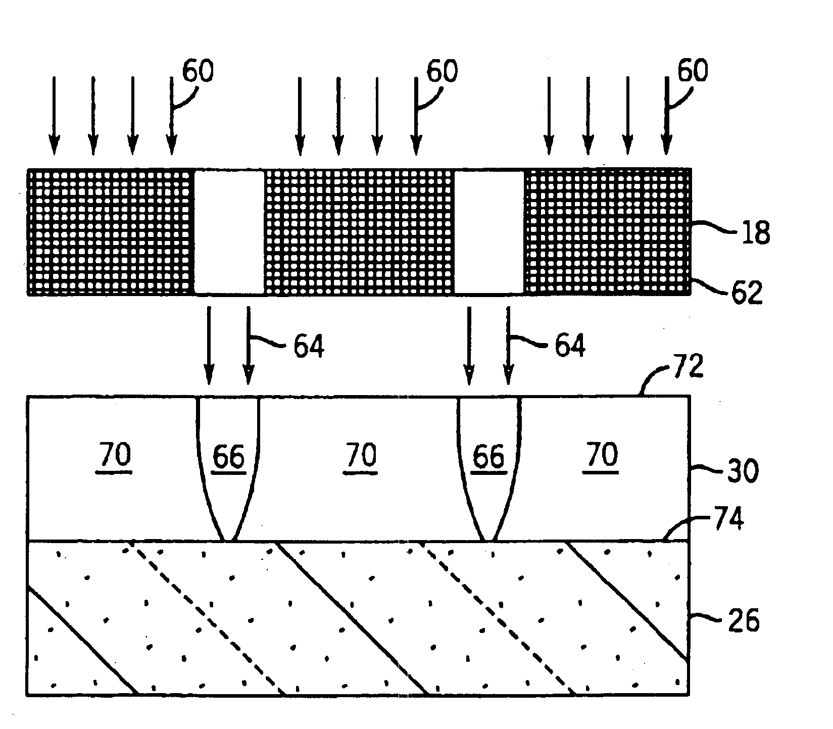
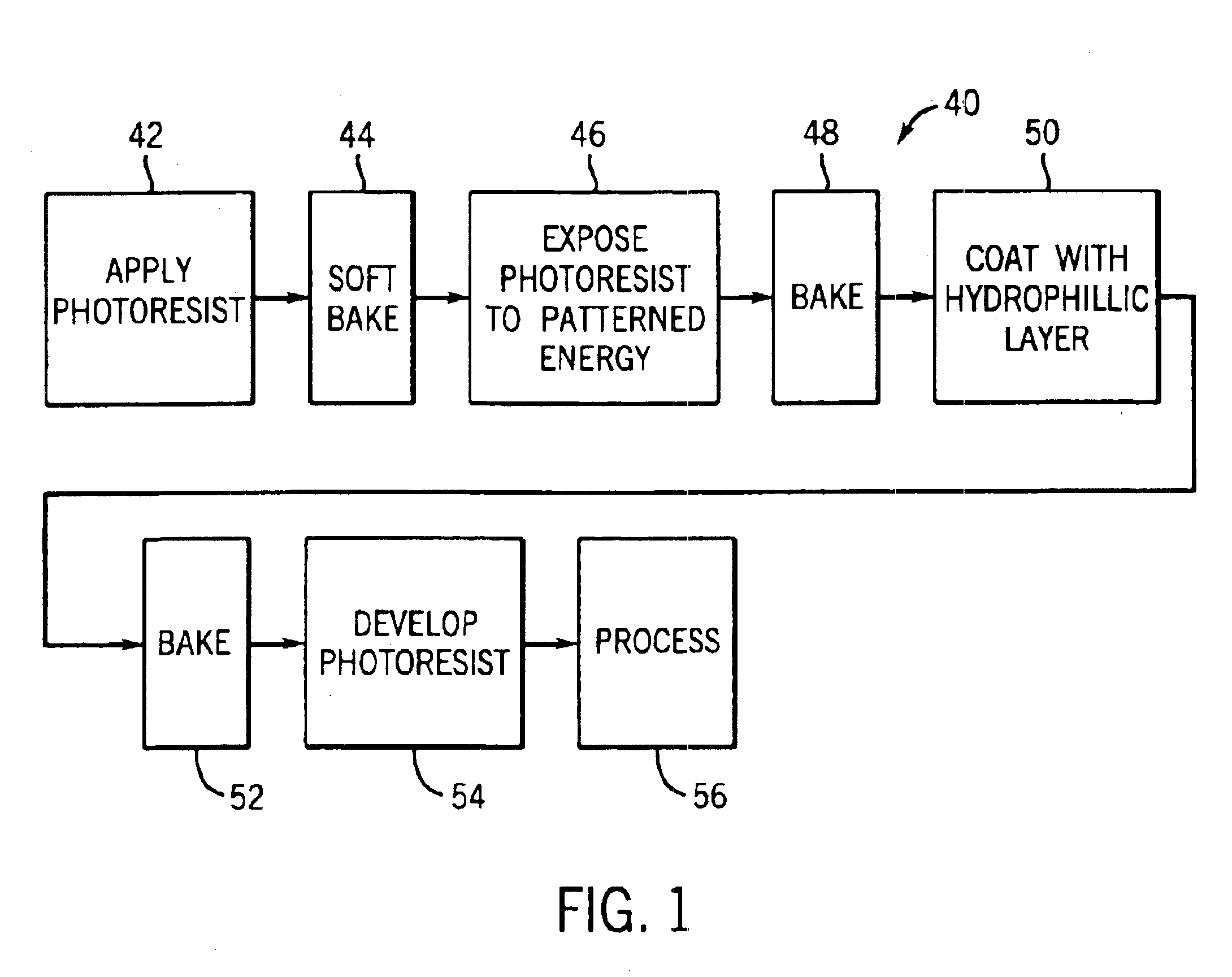
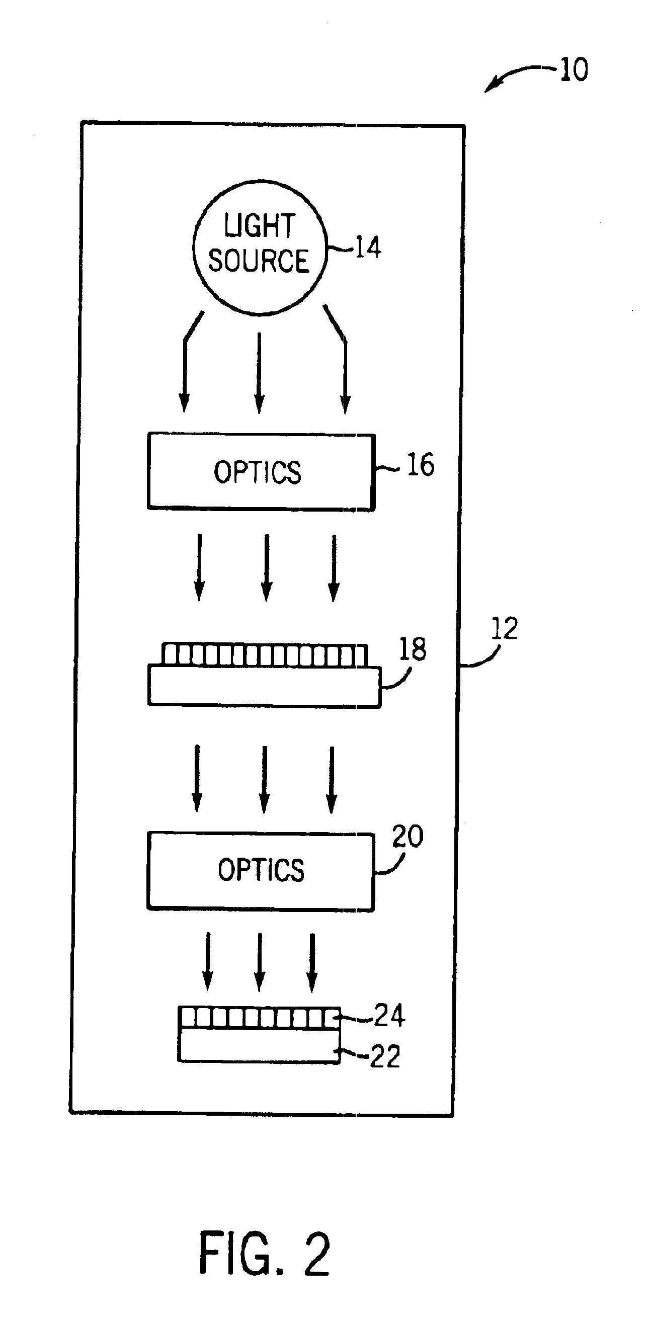
[0030]In one embodiment of the present invention, an advantageous process for forming gate features patterned on a photoresist layer is provided. The features allow gate conductors or other line structures to be formed at dimensions smaller than conventionally possible. As used in the present application, the term feature can refer to a line feature in a photoresist material, an island of photoresist material, or other lithographically formed structure associated with photoresist materials.

[0031]Preferably, the process can be implemented in an inexpensive fashion using available tools and materials. The process can be used to form extremely small (e.g., sublithographic) gate structures with wide process latitude and smooth feature side walls. Further, the process can advantageously allow for the use of low exposure dose imaging, which in turn enhances exposure tool throughput relative to conventional processes.

[0032]The advantageous process comprises exposing (e.g., treating) a phot...


PUM


Abstract

An integrated circuit fabrication process including exposing a photoresist layer and providing a hydrophilic layer above the photoresist layer. The photoresist layer is exposed to a pattern of electromagnetic energy. The polymers in the hydrophilic layer can diffuse into the photoresist layer after provision of the hydrophilic layer. The diffusion can lead to plasticization of the photoresist layer polymers in exposed regions relative to unexposed regions. The process can be utilized to form a large variety of integrated circuit structures including gate structures and other features with wide process latitude and smooth feature side walls.

Description

CROSS REFERENCE TO RELATED APPLICATIONS[0001]The present application is related to U.S. application Ser. No. 10 / 208,370 by Okoroanyanwu, entitled “Materials and Methods for Sub-Lithographic Patterning of Contact, Via, and Trench Structures in Integrated Circuit Devices,” filed on an even date herewith and assigned to the Assignee of the present application.FIELD OF THE INVENTION[0002]The present invention relates generally to integrated circuits (ICs). More particularly, the present application relates to systems for and processes of patterning of gate or other features on a layer or substrate utilized in IC fabrication.BACKGROUND OF THE INVENTION[0003]The semiconductor or integrated circuit (IC) industry aims to manufacture ICs with higher and higher densities of devices on a smaller chip area to achieve greater functionality and to reduce manufacturing costs. This desire for large scale integration requires continued shrinking of circuit dimensions and device features. The ability...

Claims


Application Information

Patent Timeline
IPC IPC(8): H01L21/02H01L21/027H01L21/28G03F7/26G03F7/38
CPCG03F7/26G03F7/38H01L21/28123H01L21/0274H01L21/0271
Inventor OKOROANYANWU, UZODINMAACHETA, ALDEN
Owner GLOBALFOUNDRIES INC
Why Eureka
Try Eureka