Display pixel having a capacitive electrode with different conductivity type from the switching element

Active Publication Date: 2005-05-03
JAPAN DISPLAY WEST
View PDF1 Cites 31 Cited by
  • Summary
  • Abstract
  • Description
  • Claims
  • Application Information

AI Technical Summary

Benefits of technology

[0076]Further, since the above structure provides a sufficient capacitance, at the time of injection of an impurity into the region of the semiconductor film for forming the auxiliary capacitance, a mask for protecting a channel forming region of the semiconductor film which region is opposed to the scanning line does not need to be removed by etching. Thus defect causing factors are reduced.
[0077]According to the present invention, a conventionally impossible structure of a switching transistor and an auxiliary capacitance is made possible, which increases the auxiliary capacitance and improves an aperture ratio.
[0078]In manufacturing the display device according to the present inven

Problems solved by technology

However, the above structure requires an independent auxiliary capacitance line, thus presenting a problem of a decrease in an aperture ratio.
This causes problems of an increase in the number of processes, a decrease in yield resulting from occurrence of defects, and the like.
The etched portion, being greatly deteriorated in terms of withstand voltage, forms a path of current leakage, and causes a defect such as a point defect or the like.
Besides, the process for removing the protective insulating film 105b is added, which represents a cost increasing factor.
Thus, with the conventional manufacturing method, a special process is requir

Method used


Image

  • Display pixel having a capacitive electrode with different conductivity type from the switching element
  • Display pixel having a capacitive electrode with different conductivity type from the switching element
  • Display pixel having a capacitive electrode with different conductivity type from the switching element

Examples


Example

First Embodiment

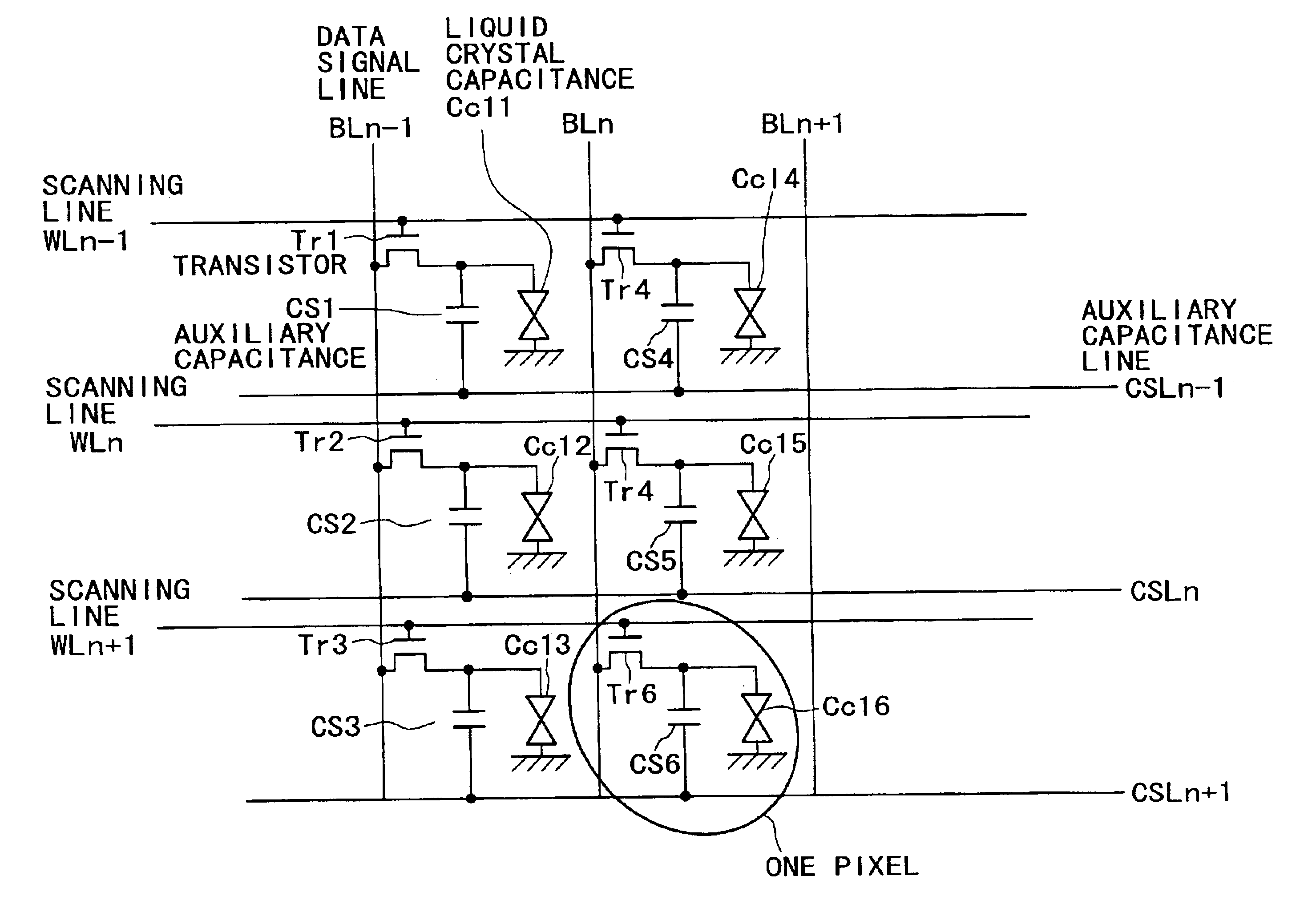
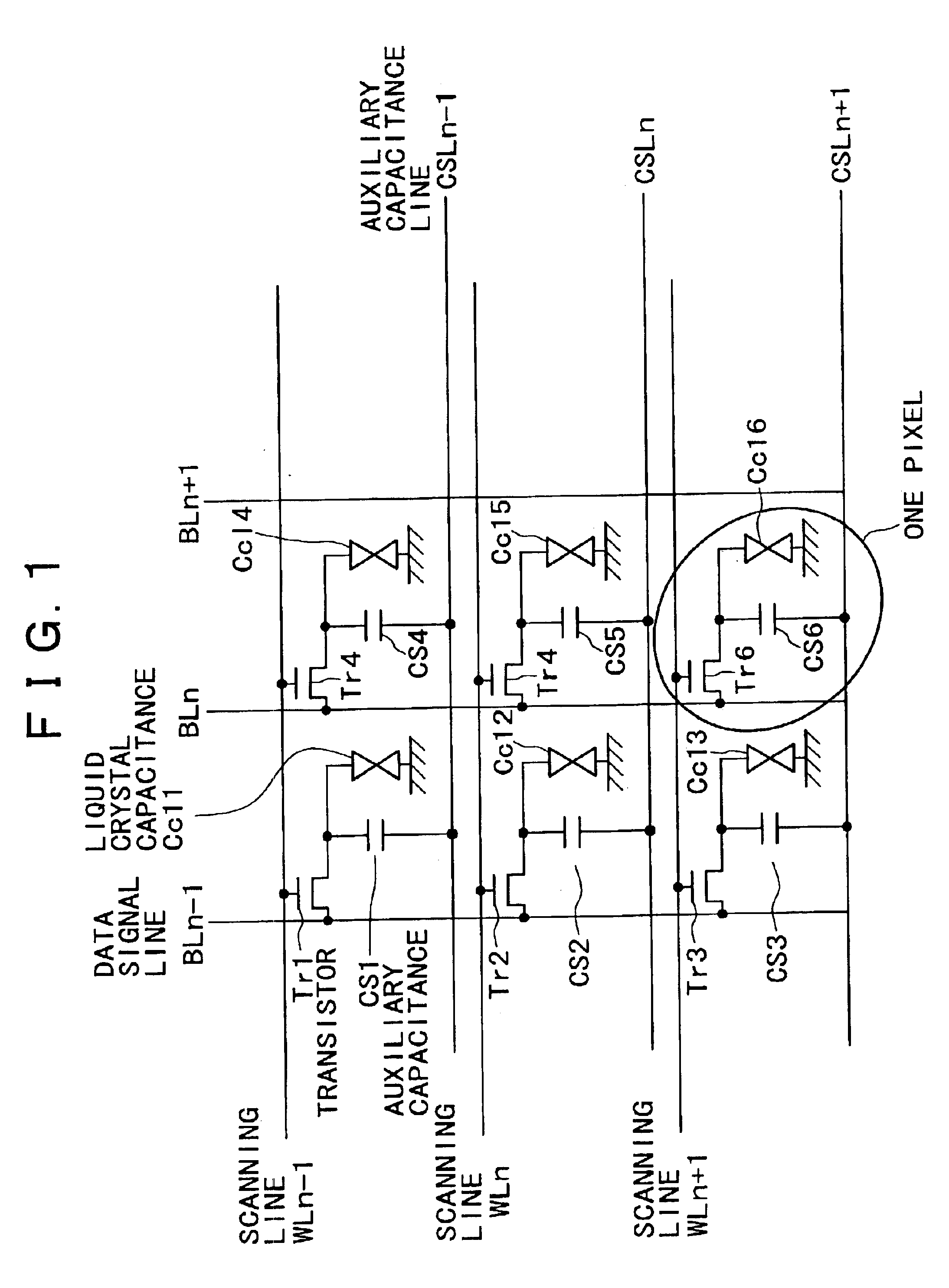
[0102]FIGS. 10A and 10B are diagrams showing an equivalent circuit and a configuration of a liquid crystal display device according to a first embodiment. The circuit arrangement diagram of FIG. 10A is similar to that of the conventional example shown in FIG. 3A. However, in FIG. 10A, a conduction type of semiconductor film possessed by auxiliary capacitances PCS1, PCS2, PCS4, and PCS5 is different from a conduction type of transistors NTr1, NTr2, NTr4, and NTr5. In this example, the transistors NTr1, NTr2, NTr4, and NTr5 are formed by an N-channel TFT, and the auxiliary MOS capacitances are formed by a P-type MOS structure. That is, the auxiliary MOS capacitances are formed by a scanning line (metal), a gate insulating film, and a P-type semiconductor film.

[0103]The conduction types may be changed to form the transistors by a P-channel type TFT and the auxiliary capacitances by an N-type MOS structure.

[0104]FIG. 10A shows an equivalent circuit of 2×2 pixels. A plura...

Example

Second Embodiment

[0143]In a second embodiment, another example of configuration of the liquid crystal display device according to the present invention will be shown.

[0144]FIG. 16 and FIG. 17 are a plan view and a schematic sectional view of the configuration of the liquid crystal display device according to the second embodiment.

[0145]The liquid crystal display device shown in FIG. 16 and FIG. 17 are basically of the same configuration as shown in FIG. 10B and FIG. 11. Therefore repeated description in the second embodiment will be omitted where appropriate, and in FIG. 16 and FIG. 17, the same references are used for the same components as in FIG. 10B and FIG. 11.

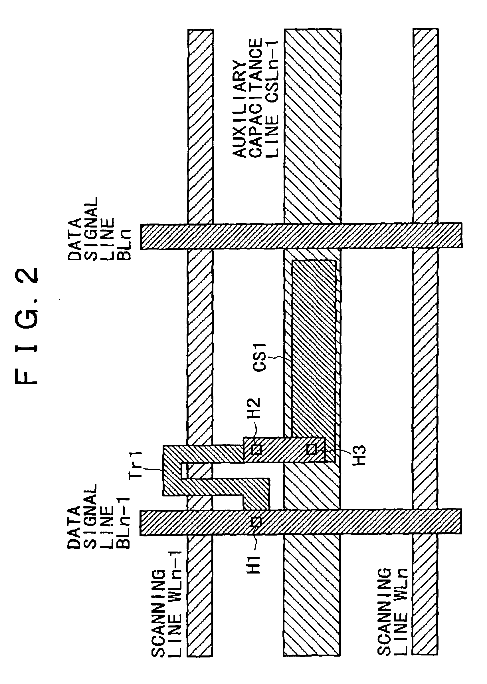
[0146]There is a difference between FIG. 16 and FIG. 10B, and between FIG. 17 and FIG. 11 in that the contact holes H2 and H3 shown in FIG. 10B for connecting the N+ type semiconductor 3 and the P+ type semiconductor 4 to each other are combined into one contact hole H4 in FIG. 16. The connecting electrode 10 shown in FIG...

Example

Third Embodiment

[0148]In a third embodiment, another example of configuration of the liquid crystal display device according to the present invention will be shown.

[0149]FIG. 18 is a plan view of the configuration of the liquid crystal display device according to the third embodiment.

[0150]In FIG. 18, the same references are used for the same components as in FIG. 16 and FIG. 11.

[0151]There is a difference between FIG. 18 and FIG. 11 and FIG. 16 in that a part of an auxiliary capacitance PCS1 in FIG. 18 is disposed under a data signal line BLn−1.

[0152]In this case, a region required for forming the necessary auxiliary capacitance is formed in a region where light does not pass through originally, for example a metal region (data signal line in this case). Therefore a loss in transmittance becomes smaller, and thus a high aperture ratio can be secured.

[0153]Either of a bottom gate type transistor structure and a top gate type transistor structure may be formed in this case.

[0154]When...


PUM


Abstract

Disclosed herein is a display device, including a display element, a first scanning line, a second scanning line, a data signal line, a switching element having a first terminal and a second terminal of a first conduction type, the first terminal being connected to the data signal line, for being held in a conducting state or a non-conducting state according to a voltage applied to the first scanning line, and a storage capacitance having a first electrode and a second electrode that shares the second scanning line, wherein the second terminal of the switching element is connected to the display element and connected to the first electrode of the storage capacitance including a semiconductor film of a second conduction type different from the second terminal.

Description

BACKGROUND OF THE INVENTION[0001]The present invention relates to a display device and a method of manufacturing the same, and particularly to a liquid crystal display device and a method of manufacturing the same.[0002]With characteristics of being thin and low power consumption, liquid crystal display devices are widely used in notebook computers, display devices for car navigation, personal digital assistants (PDAs), portable telephones and the like. The liquid crystal display device is roughly classified into a transmissive type that controls light from a backlight for display, a reflective type that reflects extraneous light such as sunlight or the like for display, or a recent display device referred to as a transflective type that combines characteristics of both the transmissive type and the reflective type.[0003]Applications of these display devices require that the display devices consume low power, and therefore a high aperture ratio is required to maximize efficiency of ...

Claims


Application Information

Patent Timeline
IPC IPC(8): G02F1/13G02F1/1362G02F1/1368G02F1/1343G09F9/30H01L21/336H01L29/786
CPCG02F1/136213H01L27/1255G02F1/1368G02F1/136
Inventor TANAKA, TSUTOMU
Owner JAPAN DISPLAY WEST
Why Eureka
Try Eureka