Method and circuit for reducing DRAM refresh power by reducing access transistor sub threshold leakage

a technology of access transistor and refresh power, which is applied in the direction of information storage, static storage, digital storage, etc., can solve the problems of increasing the power consumption of memory devices with both the capacity and the operating speed of memory devices, and affecting the length of time they can be used, so as to reduce the required refresh rate of dram and achieve good positive voltage regulation. , the effect of reducing the required refresh ra

Inactive Publication Date: 2005-05-03
NAN YA TECH
View PDF30 Cites 20 Cited by
  • Summary
  • Abstract
  • Description
  • Claims
  • Application Information

AI Technical Summary

Benefits of technology

[0018]In accordance with the present invention, an n-sense amplifier is powered with a relatively small positive voltage so that the sense amplifier can maintain digit lines at the positive voltage rather than at zero volts. As a result, the sub threshold leakage current of access transistors in a DRAM is reduced to reduce the required refresh rate of the DRAM. Significantly, the positive voltage is supplied by a voltage regulator using bipolar transistors, which are easily able to provide good regulation of the positive voltage applied to the n-sense amplifier. The bipolar transistor voltage regulator is fabricated in an isolated p-well so that the base voltage of the bipolar transistor can be controlled by controlling the local substrate voltage. The isolated p-well is preferably fabricated by a triple well formed by an n-type implantation and n-type wells in a p-type substrate.

Problems solved by technology

For example, the power consumed by memory devices used in portable personal computers greatly affects the length of time they can be used without the need to recharge batteries powering such computers.
Power consumption can also be important where memory devices are not powered by batteries because it may be necessary to limit the heat generated by the memory devices.
In general, the power consumption of memory devices increases with both the capacity and the operating speed of memory devices.
The power consumed by memory devices is also affected by their operating mode.
A dynamic random access memory (“DRAM”), for example, will generally consume a relatively large amount of power when the memory cells of the DRAM are being refreshed.
Each time a row of memory cells is actuated, a pair of digit lines for each memory cell are switched to complementary voltages and then equilibrated, thereby consuming a significant amount power.
Power consumption also increases with increases in the rate at which the rows of memory cells are actuated.
Therefore, if the required refresh rate for a DRAM could be reduced, so also could the refresh power consumption.
The result is an erroneous reading of the memory cell 100 known as a data retention error.
While this approach successfully reduces the sub-threshold leakage current of the access transistors 120 and consequently reduces the required refresh rate, it creates other problems for the DRAMs.
For example, since charge pumps are inherently very inefficient in converting one voltage to another, the need for a charge pump can unduly increase the power consumption of a DRAM.
Also, negatively biasing the entire substrate in which the DRAM is fabricated can cause other circuitry, such as output buffers for the DRAM, to “lock up” and pull the voltage of the substrate to a positive voltage, such as VCC.
When this happens, the DRAM becomes inoperative.
Although this approach does reduce the power consumed by a negative voltage charge pump and does prevent other circuitry from being affected by the negative substrate voltage, it creates other problems.
As a result, DRAMs using this approach must be relatively large, which adversely affects the cost and operating speed of such DRAMs.
This can be a considerable period, e.g., up to 120 MS., because data may be read sequentially from each column of an active row, which can require considerable time.
However, these techniques create other problems that can impair the performance and / or expense of DRAMs.
Unfortunately, it is difficult to achieve precise control of voltages with MOSFET transistors typically used in DRAMs.
As a result, this approach to has not met with much practical success.

Method used


Image

  • Method and circuit for reducing DRAM refresh power by reducing access transistor sub threshold leakage
  • Method and circuit for reducing DRAM refresh power by reducing access transistor sub threshold leakage
  • Method and circuit for reducing DRAM refresh power by reducing access transistor sub threshold leakage

Examples


Embodiment Construction

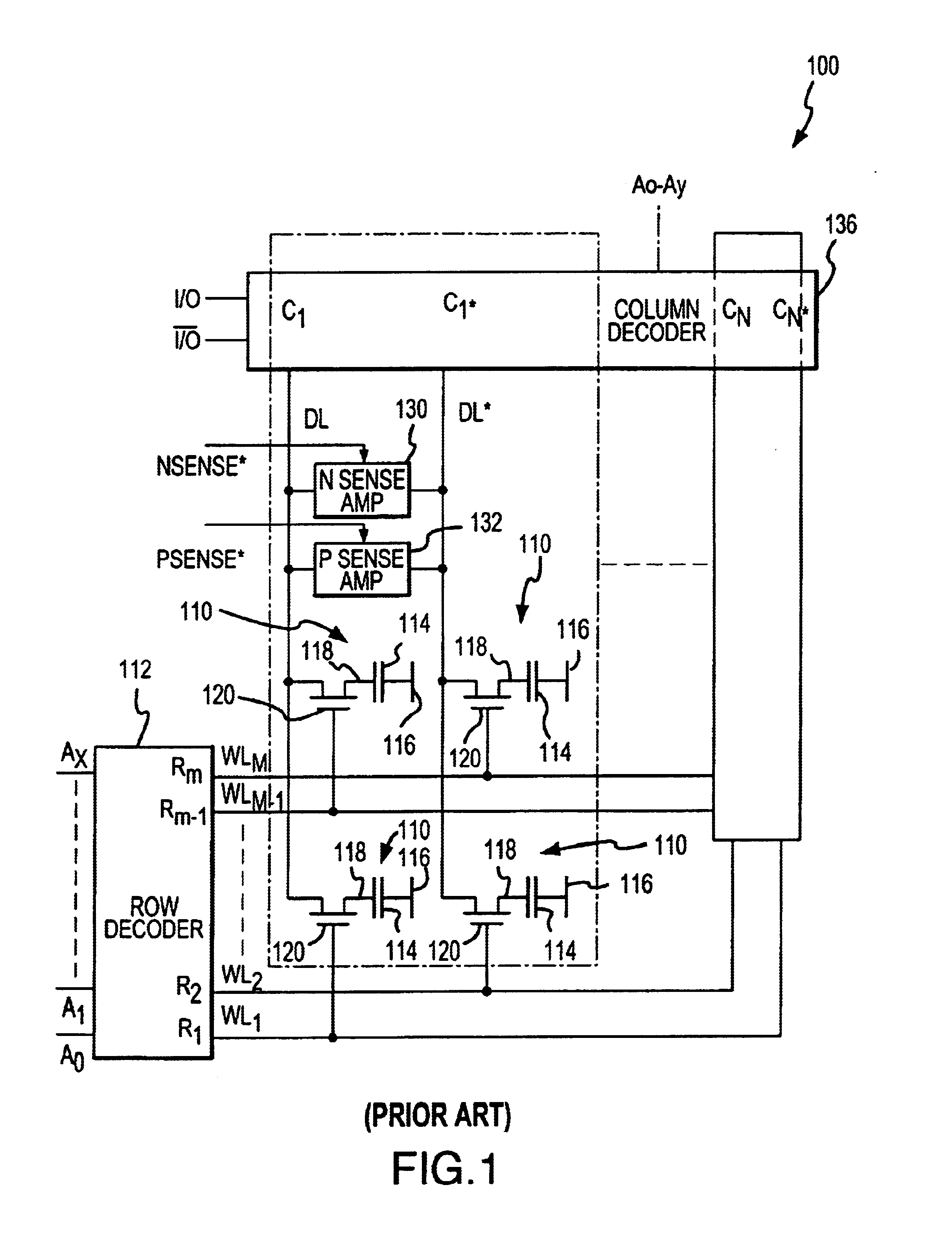
[0029]A portion of a memory array 160 according to one example of the invention is shown in FIG. 3. The memory array 160 is identical to the memory array 100 shown in FIG. 1, except for differences that will be discussed below. Therefore, in the interest of clarity and brevity, identical components have been provided with the same reference designations, and an explanation of their structure and operation will not be repeated. The memory array 160 differs from the memory array 100 by including a bipolar transistor voltage regulator 170 to provide a small positive voltage VOUT to power the n-sense amplifiers 130 responsive to receiving the NSENSE* signal that is normally applied directly to the n-sense amplifiers. As a result, as previously explained, the n-sense amplifiers 130 drive the digit lines DL to a small positive voltage, rather than zero volts, to decrease the sub threshold leakage currents of the access transistors for the inactive rows. In one example of the invention, th...


PUM


Abstract

The required refresh rate of a DRAM is reduced by biasing active digit lines to a slight positive voltage to reduce the sub threshold current leakage of access transistors in memory cells that are not being accessed. The slight positive voltage is provided by a voltage regulator circuit using one or more bipolar transistors fabricated in a well that electrically isolates the bipolar transistors from the remainder of the substrate. The voltage provided by the voltage regulator is preferably coupled to the access transistors by powering each of the n-sense amplifiers in the DRAM with the voltage from the voltage regulator.

Description

TECHNICAL FIELD[0001]The invention relates dynamic random access memory (“DRAM”) devices, and, more particularly, to a circuit and method for reducing the sub threshold current leakage through DRAM access transistors thereby reducing the required refresh rate.BACKGROUND OF THE INVENTION[0002]The power consumed by integrated circuits can be a critical factor in their performance in certain applications. For example, the power consumed by memory devices used in portable personal computers greatly affects the length of time they can be used without the need to recharge batteries powering such computers. Power consumption can also be important where memory devices are not powered by batteries because it may be necessary to limit the heat generated by the memory devices.[0003]In general, the power consumption of memory devices increases with both the capacity and the operating speed of memory devices. The power consumed by memory devices is also affected by their operating mode. A dynami...

Claims


Application Information

Patent Timeline
Patent Type & Authority Patents(United States)
IPC IPC(8): G11C11/406
CPCG11C11/406G11C2211/4068G11C2211/4067G11C2211/4061
Inventor KIRSCH, HOWARD C.
Owner NAN YA TECH
Why Eureka
Try Eureka