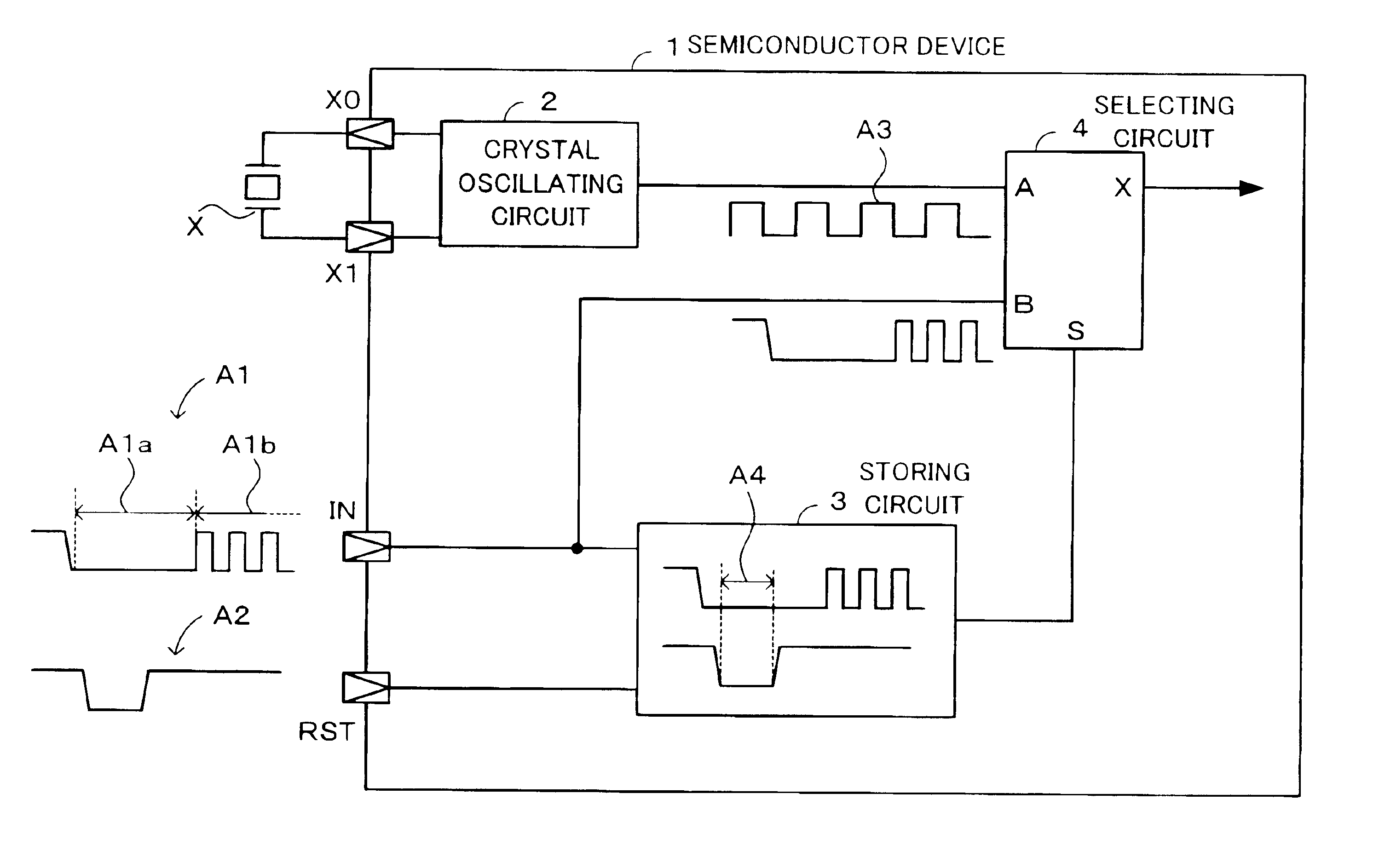
Semiconductor device
a technology of semiconductor devices and components, applied in the direction of instruments, generating/distributing signals, pulse techniques, etc., can solve the problems of increasing the number of necessary components and mounting areas, and supplying the corresponding clock with the frequency of the inputted clock, so as to increase the number of terminals
- Summary
- Abstract
- Description
- Claims
- Application Information
AI Technical Summary
Benefits of technology
Problems solved by technology
Method used
Image

Examples
first embodiment
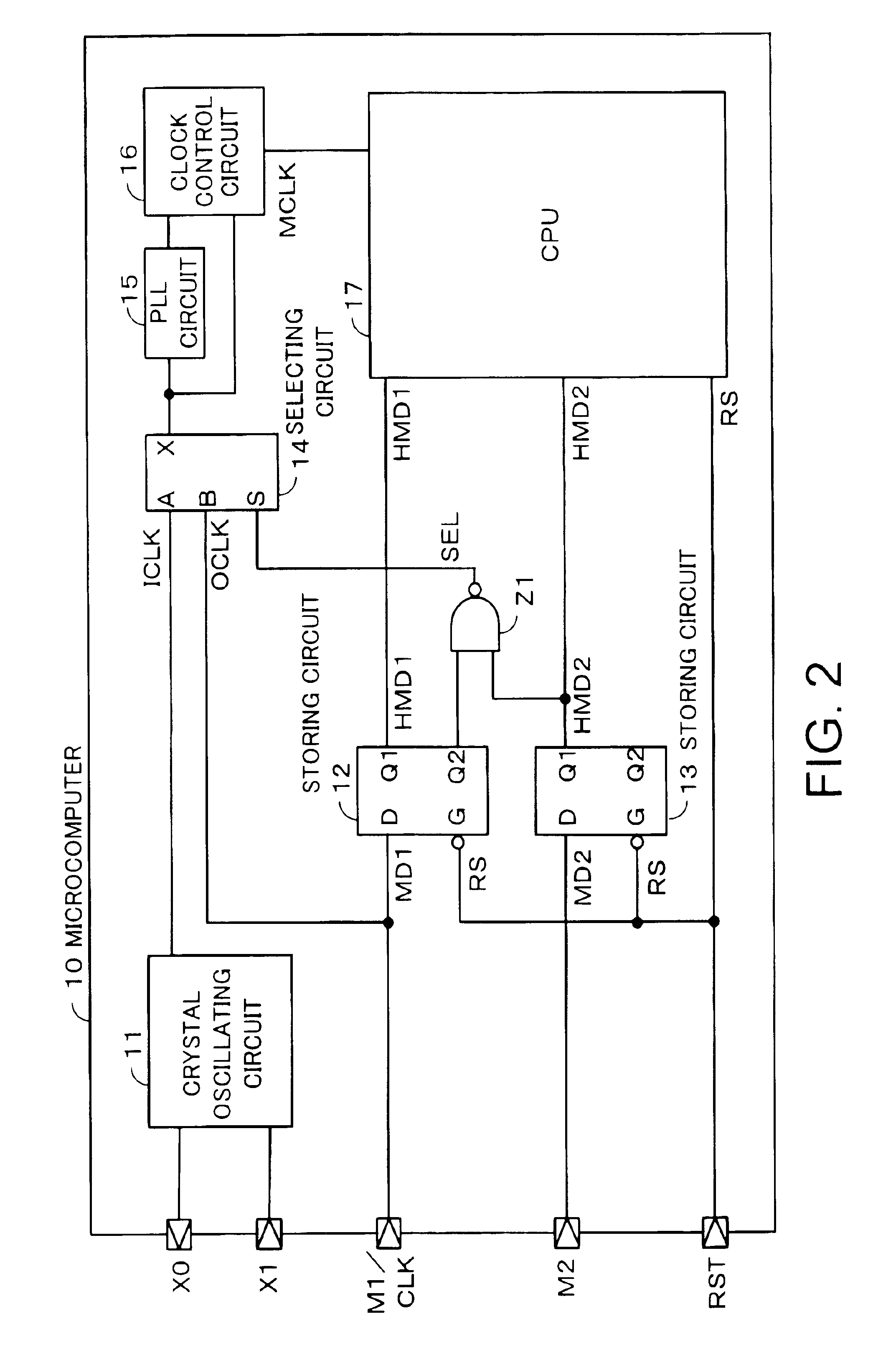
[0046]FIG. 2 is a circuit diagram showing a microcomputer according to the present invention. The microcomputer 10 includes a crystal oscillating circuit 11, storing circuits 12 and 13, a NAND circuit Z1, a selecting circuit 14, a PLL (Phase Locked Loop) circuit 15, a clock control circuit 16, and a CPU 17. It further includes the crystal oscillating terminals X0 and X1, a mode / external clock terminal M1 / CLK, a mode terminal M2, and the reset RST.
[0047]The crystal oscillating terminals X0 and X1 are to be connected with the crystal oscillator.
[0048]The mode / external clock terminal M1 / CLK is a terminal to which are to be inputted a mode signal MD1 for indicating whether the external clock is to be used and the external clock OCLK on which the CPU 17 is operated by synchronous mode. The mode signal MD1 is also inputted into the CPU 17 for defining the operation mode of the CPU 17.
[0049]The reset terminal RST is a terminal into which the reset signal RS for resetting (initializing) the...
second embodiment
[0087]In turn, the description will be oriented to the present invention.
[0088]FIG. 6 is a circuit diagram showing a microcomputer according to a second embodiment of the present invention. Unlike the microcomputer 10 of the first embodiment, the microcomputer 30 is arranged so that the output of the NAND circuit Z1 is inputted into the crystal oscillating circuit 11. The same components as those of the first embodiment have the same reference numbers. The description about those components is left out.
[0089]The crystal oscillating circuit 11 is composed of FET transistors Q1 and Q2, an inverter circuit Z2, a NAND circuit Z3, and a Schmitt trigger circuit Z4.
[0090]The FET transistor Q1 is an n-channel FET transistor. When the H signal is inputted into the gate of the transistor Q1, the transistor Q1 connects the source with the drain. The FET transistor Q2 is a p-channel FET transistor. When the L signal is inputted into the gate of the transistor Q2, the transistor Q2 connects the ...
third embodiment
[0107]In turn, the description will be oriented to the present invention.
[0108]FIG. 8 is a circuit diagram showing a microcomputer according to the third embodiment of the present invention. The microcomputer 40 includes a NOR circuit Z5 and an AND circuit Z6 in addition to the microcomputer 30 of the second embodiment. The same components as those of the second embodiment have the same reference numbers. The description about those components is left out.
[0109]In order to suppress the power consumption, the CPU 17 starts execution of a program for stopping the supply of the operation clock MCLK, when the H stop signal ST is outputted.
[0110]One input of the NOR circuit Z5 is connected with the output of the NAND circuit Z1 and the other input of the circuit Z5 is connected with a signal line to which the CPU 17 outputs the stop signal ST. The output of the NOR circuit Z5 is connected with the input of the inverter circuit Z2 of the crystal oscillating circuit 11.
[0111]When the selec...
PUM
 Abstract
Description
Claims
Application Information
 - R&D
- Intellectual Property
- Life Sciences
- Materials
- Tech Scout
- Unparalleled Data Quality
- Higher Quality Content
- 60% Fewer Hallucinations
Browse by: Latest US Patents, China's latest patents, Technical Efficacy Thesaurus, Application Domain, Technology Topic, Popular Technical Reports.
© 2025 PatSnap. All rights reserved.Legal|Privacy policy|Modern Slavery Act Transparency Statement|Sitemap|About US| Contact US: help@patsnap.com