Flash memory with trench select gate and fabrication process

a technology of flash memory and select gate, which is applied in the direction of digital storage, instruments, transistors, etc., can solve the problems of limiting the utility of the stack-gate cell, and affecting the efficiency of the flash memory

Inactive Publication Date: 2005-05-17
SILICON STORAGE TECHNOLOGY
View PDF9 Cites 160 Cited by
  • Summary
  • Abstract
  • Description
  • Claims
  • Application Information

AI Technical Summary

Benefits of technology

[0011]It is in general an object of the invention to provide a new and improved flash memory and process for fabricating the same.

Problems solved by technology

However, a stack-gate cell has an over-erase problem which a split-gate cell does not have.
This problem is commonly addressed by maintaining the threshold voltage of the cell in a range of about 1.0-2.0 volts after an erase cycle, which adds complexity to the circuit design.
Even though this approach permits in a smaller cell size than the widely used ETOX technology, the need for a select gate in addition to the stacked control and floating gates limits its utility as cell sizes continue to decrease toward hundreds of nanometers.

Method used


Image

  • Flash memory with trench select gate and fabrication process
  • Flash memory with trench select gate and fabrication process
  • Flash memory with trench select gate and fabrication process

Examples


Embodiment Construction

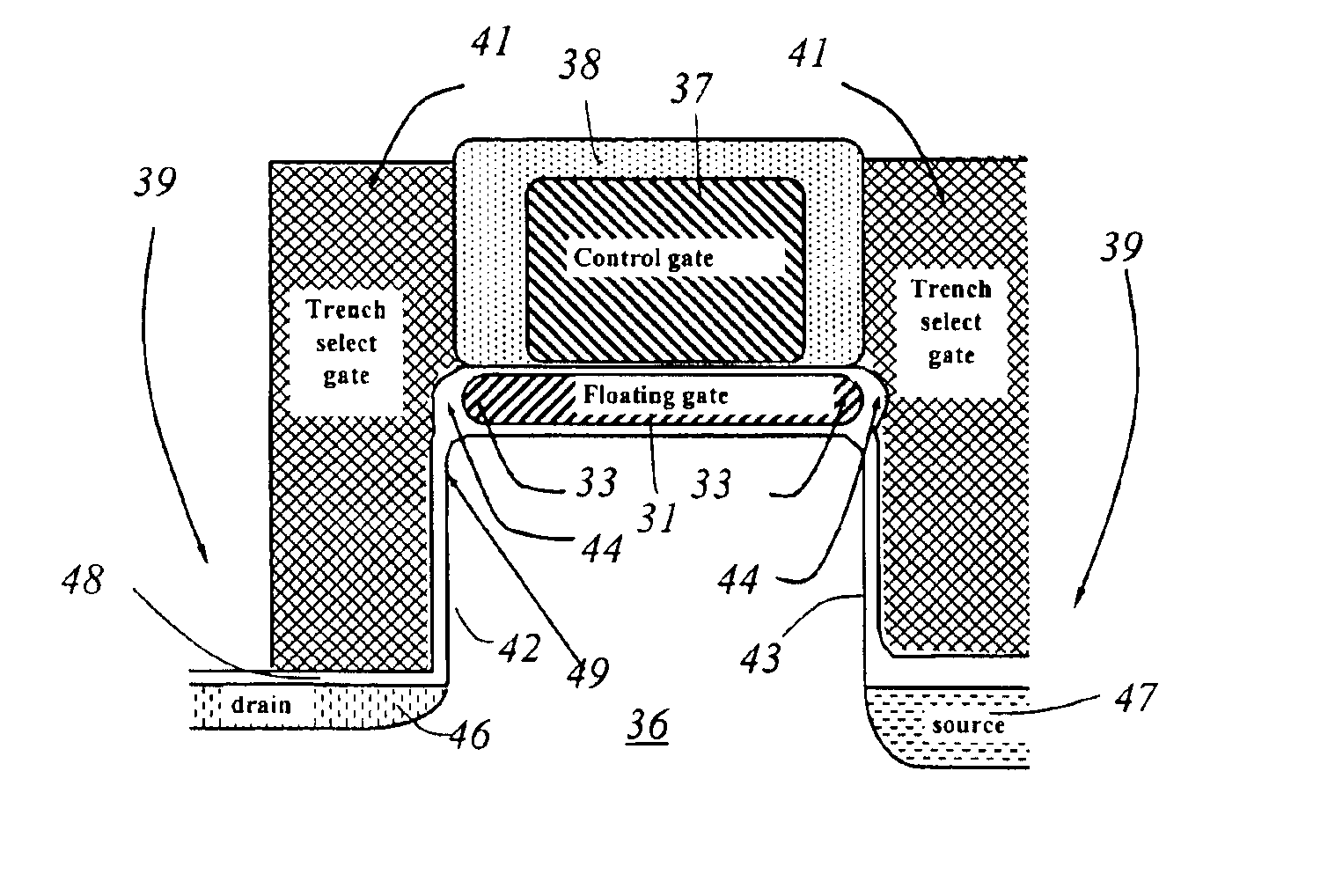
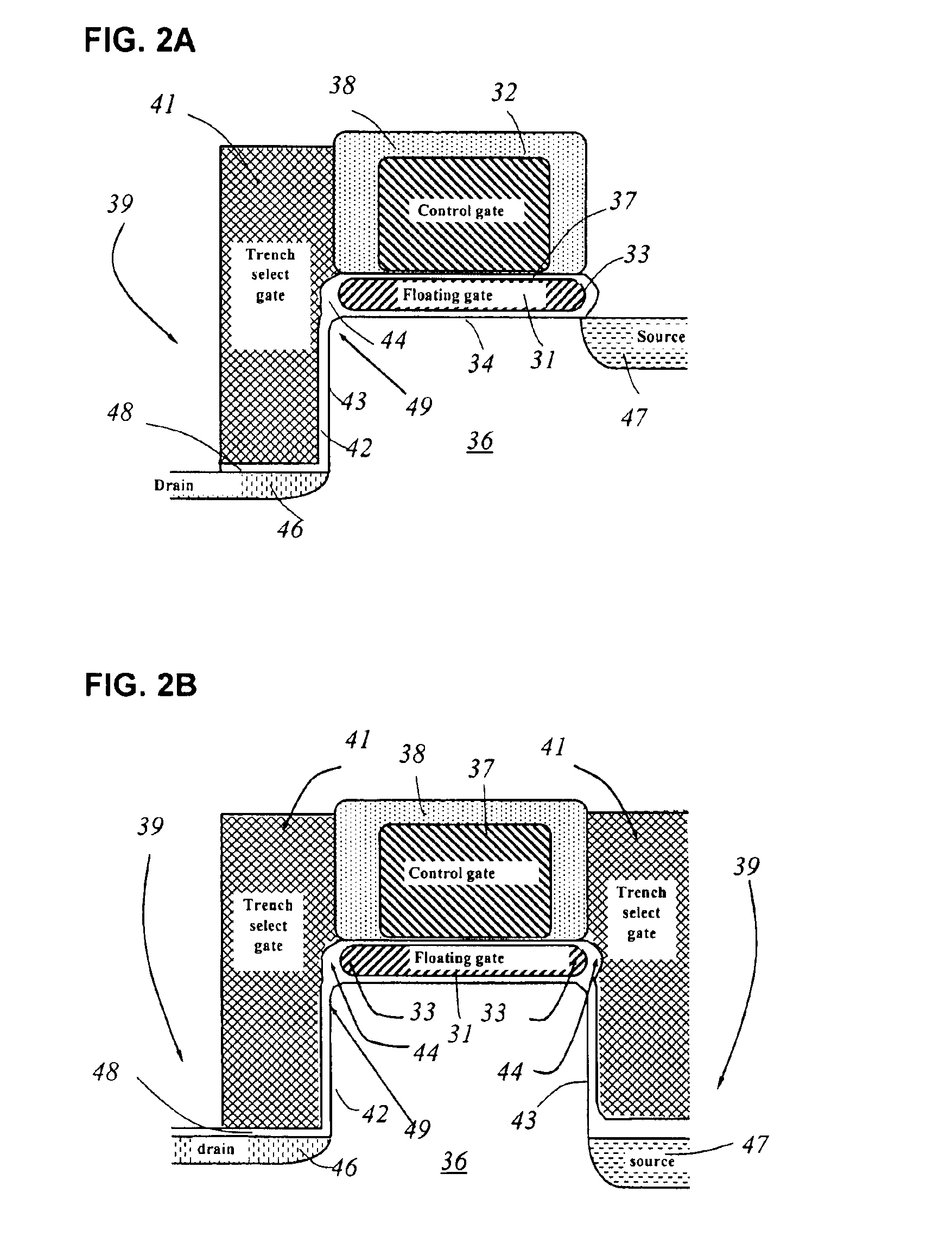
[0025]As illustrated in FIG. 2A, the memory cell has a floating gate 31 and a control gate 32, with the control gate being positioned above and in vertical alignment with the floating gate.

[0026]The floating gate is fabricated of a conductive material such as polysilicon or amorphous silicon, with a preferred thickness on the order of 100 Å to 1000 Å and sharply curved side walls 33. A thin gate insulator 34, typically a thermal oxide, separates the floating gate from the silicon substrate 36 beneath it.

[0027]The control gate is narrower in horizontal dimension and thicker in vertical dimension than the floating gate, with the edges of the floating gate extending laterally beyond the edges of the control gate. The control gate is fabricated of a conductive material such as a doped polysilicon or polycide, and it is insulated from the floating gate beneath it by a dielectric film 37. That film can be either a pure oxide or a combination of oxide, nitride and oxide (ONO), and in one p...


PUM


Abstract

Flash memory and process of fabrication in which memory cells are formed with select gates in trenches between stacked, self-aligned floating and control gates, with buried source and drain regions which are gated by the select gates. Erase paths are formed between projecting rounded edges of the floating gates and the select gates, and programming paths extend from the mid-channel regions between the select gates and floating gates through the gate oxide to the edges of the floating gates. Trenched select gates can be provided on one or both sides of the floating and control gates, depending upon array architecture, and the stacked gates and dielectric covering them are used as a self-aligned mask in etching the substrate and other materials to form the trenches.

Description

BACKGROUND OF THE INVENTION[0001]1. Field of Invention[0002]This invention pertains generally to semiconductor memory devices and, more particularly, to a self-aligned split-gate flash memory and process of fabricating the same.[0003]2. Related Art[0004]Nonvolatile memory is currently available in several forms, including electrically programmable read only memory (EPROM), electrically erasable programmable read only memory (EEPROM), and flash EEPROM. Flash memory has been widely used for high volume data storage in devices such as memory cards, personal digital assistants (PDA's) and MP3 players. Such applications require high density memory, with smaller cell size and reduced cost of manufacture.[0005]In general, there are two basic types of nonvolatile memory cell structures: stack-gate and split-gate. The stack-gate memory cell usually has a floating gate and a control gate, with the control gate being positioned directly above the floating gate. In a split-gate cell the control...

Claims


Application Information

Patent Timeline
Patent Type & Authority Patents(United States)
IPC IPC(8): H01L29/76G11C11/34G11C16/04H01L27/115H01L21/70H01L29/66H01L21/8239H01L21/8247H01L29/788H01L27/105H01L21/28H01L21/336H01L29/423
CPCG11C16/0433H01L21/28273H01L27/115H01L29/66825H01L29/42328H01L29/42336H01L27/11521H01L29/40114H10B69/00H10B41/30
Inventor FAN, DER-TSYRLU, JUNG-CHANGCHEN, CHIOU-FENGTUNTASOOD, PRATEEP
Owner SILICON STORAGE TECHNOLOGY
Why Eureka
Try Eureka