Interconnection and input/output resources for programmable logic integrated circuit devices

a technology of integrated circuit devices and input/output resources, which is applied in the direction of computation using denominational number representation, pulse techniques, instruments, etc., can solve the problems of increasing the size of the die, increasing difficult to significantly further reduce the longest signal propagation time, so as to increase the speed of all the interconnection resources, double the speed at which the device can be clocked, and halve the propagation time of the signal

Inactive Publication Date: 2005-05-17
ALTERA CORP
View PDF92 Cites 6 Cited by
  • Summary
  • Abstract
  • Description
  • Claims
  • Application Information

AI Technical Summary

Benefits of technology

[0011]A typical design objective for the high-speed resources is to make it possible to double the speed at which the device can be clocked by providing a sufficient quantity of sufficiently fast high-speed resources so that those resources can be used to convey the signals that give the device its longest signal propagation time and to thereby halve the propagation time of those signals. On the other hand, to avoid the disadvantages of simply trying to greatly increase the speed of all the interconnection resources on the device, only a minor portion of the interconnection resources of any given kind are made high-speed. The major portion remain normal-speed and are used for the bulk of the interconnections that are less speed-critical.
[0012]The input/output (“I/O”) circuitry of PLDs may be improved in accordance with the invention

Problems solved by technology

A PLD cannot be safely clocked at a clock rate having a period less than this longest signal propagation time.
Once this has been done, however, for a given integrated circuit fabrication technology, it is dif

Method used


Image

  • Interconnection and input/output resources for programmable logic integrated circuit devices
  • Interconnection and input/output resources for programmable logic integrated circuit devices
  • Interconnection and input/output resources for programmable logic integrated circuit devices

Examples


Embodiment Construction

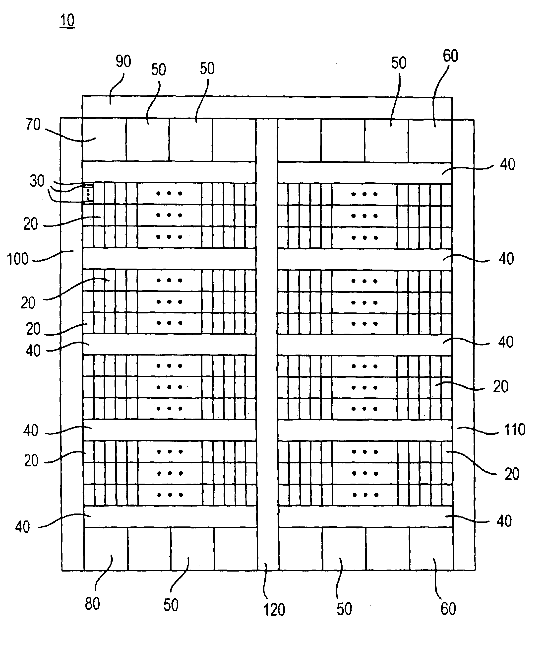
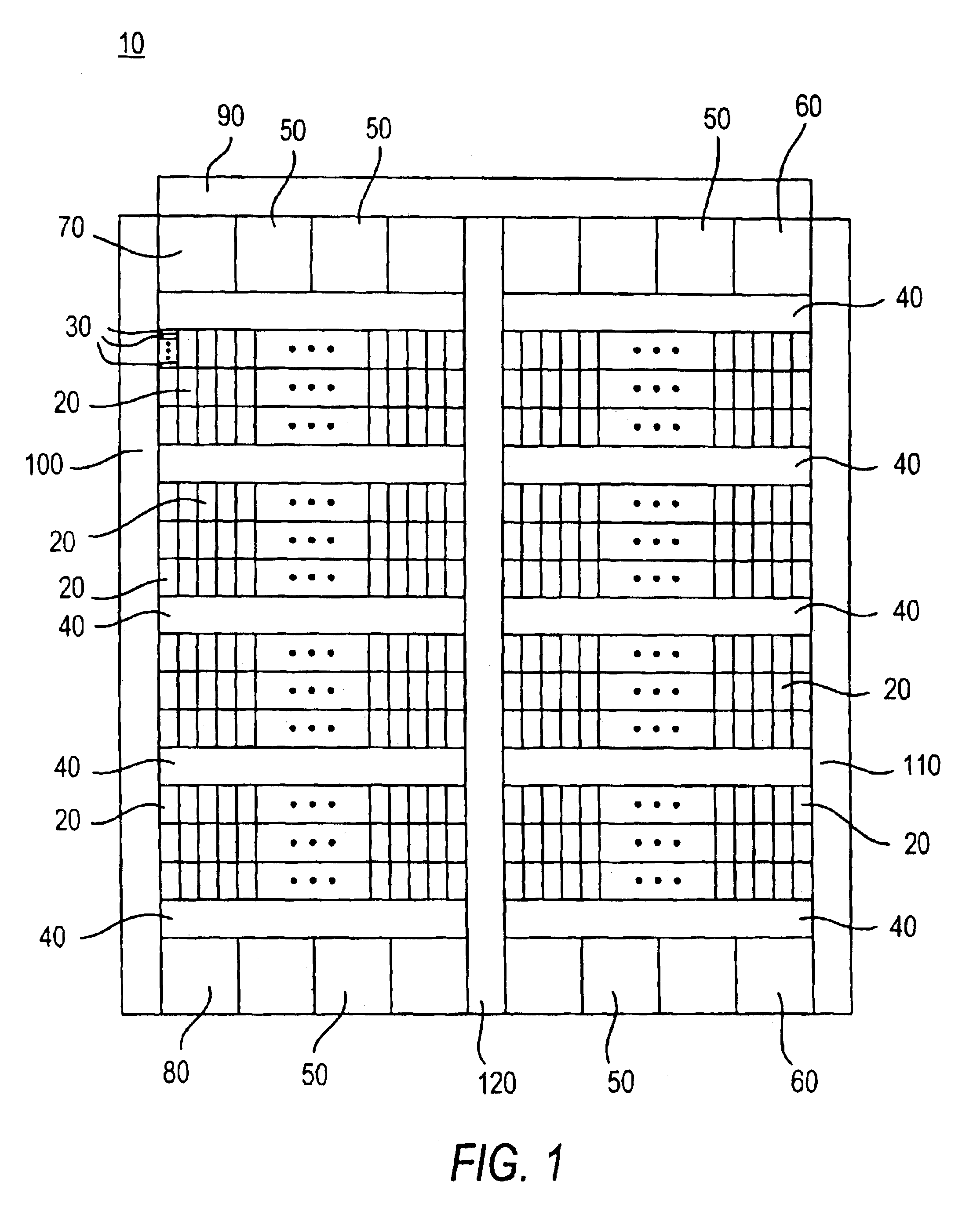
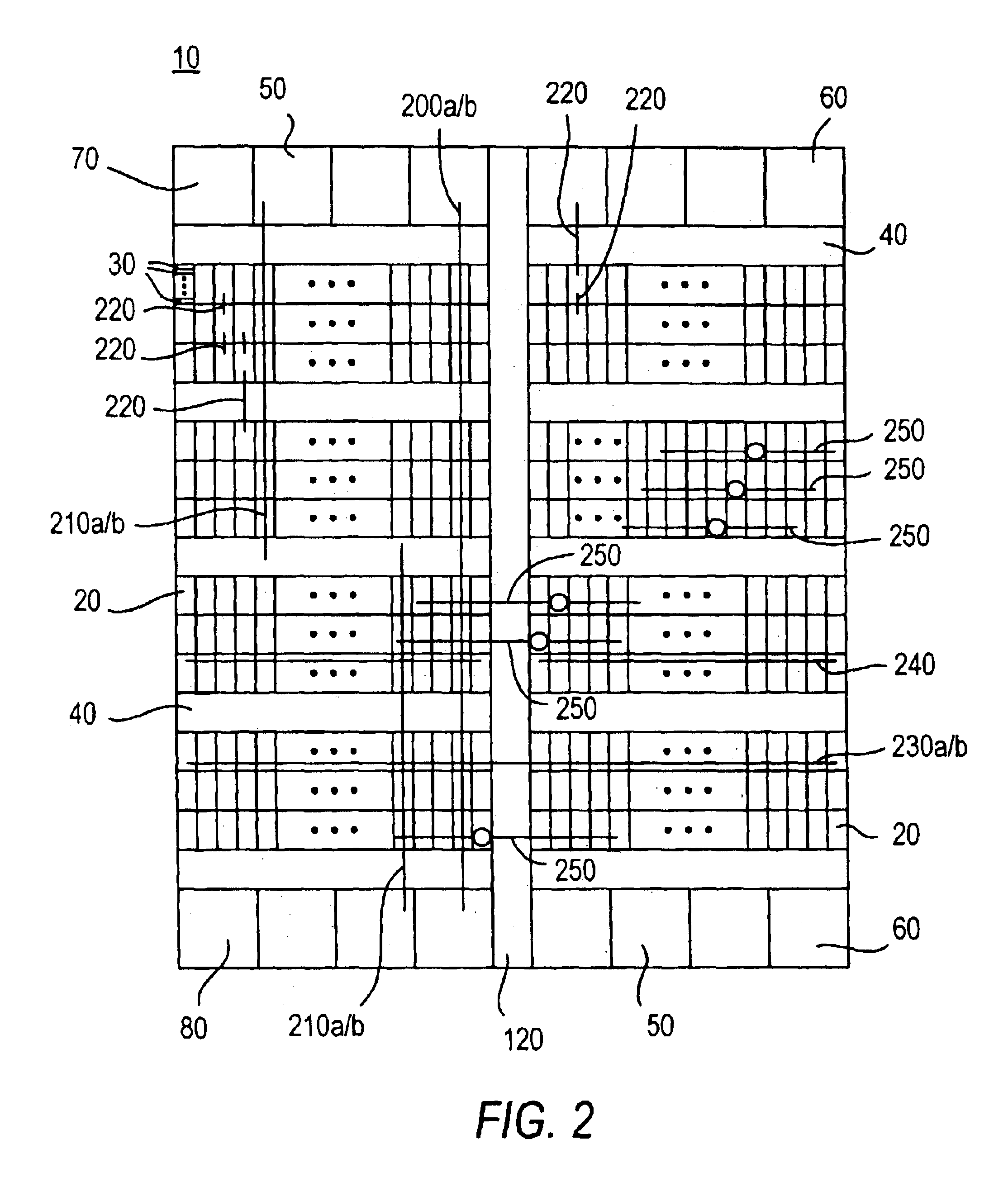
[0027]An illustrative programmable logic device 10, which can be constructed in accordance with this invention, is shown in FIG. 1. Device 10 includes 12 rows of regions 20 of programmable logic. Each row includes 40 regions 20. Thus regions 20 are disposed on device 10 in a two-dimensional array of 12 rows intersecting 40 columns of regions 20.

[0028]Each region 20 includes ten subregions 30 of programmable logic. To avoid over-complicating FIG. 1, the individual subregions 30 are delineated only in the extreme upper-left-hand region 20. As will explained more fully later in this specification, each subregion 30 is programmable by a user of device 10 to perform any of several relatively small logic functions. Extremely complex logic functions can be performed by concatenating subregions 30 via a programmable network of interconnection conductors and other associated interconnection resources on device 10.

[0029]Interspersed among the rows of regions 20 are five rows of input / output (...


PUM


Abstract

A programmable logic integrated circuit device has a plurality of regions of programmable logic disposed on the device in a plurality of intersecting rows and columns of such regions. Interconnection resources (e.g., interconnection conductors, signal buffers/drivers, programmable connectors, etc.) are provided on the device for making programmable interconnections to, from, and/or between the regions. At least some of these interconnection resources are provided in two forms that are architecturally similar (e.g., with similar and substantially parallel routing) but that have significantly different signal propagation speed characteristics. For example, a major or larger portion of such dual-form interconnection resources may have what may be termed normal signal speed, while a smaller minor portion may have significantly faster signal speed. Secondary (e.g., clock and clear) signal distribution may also be enhanced, and so may be input/output circuitry and cascade connections between adjacent or nearby logic modules on the device.

Description

[0001]This application is a divisional of U.S. patent application Ser. No. 10 / 047,618, filed Jan. 14, 2002, now U.S. Pat. No. 6,614,261, which is a divisional of U.S. patent application Ser. No. 09 / 516,921, filed Mar. 2, 2000, now U.S. Pat. No. 6,407,576; which claims the benefit of the following U.S. provisional patent applications: No. 60 / 122,788, filed Mar. 4, 1999; No. 60 / 142,431, filed Jul. 6, 1999; No. 60 / 142,508, filed Jul. 6, 1999; and U.S. No. 60 / 142,513, filed Jul. 6, 1999. All of these prior applications are hereby incorporated by reference herein in their entireties.BACKGROUND OF THE INVENTION[0002]This invention relates to programmable logic array integrated circuit devices (“programmable logic devices” or “PLDs”), and more particularly to interconnection resources for use on programmable logic devices that increase the speed at which those devices can be made to operate. The invention also relates to such other features of PLDs as secondary signal (e.g., clock and clea...

Claims


Application Information

Patent Timeline
IPC IPC(8): G06F7/50G06F7/48H03K19/177H03K19/173G06F7/506
CPCG06F7/506H03K19/1737H03K19/177H03K19/17792H03K19/17736H03K19/1774H03K19/17744H03K19/17728
Inventor NGAI, TONYPEDERSEN, BRUCESHUMARAYEV, SERGEYSCHLEICHER, JAMESHUANG, WEI-JENHUTTON, MICHAELMARURI, VICTORPATEL, RAKESHKAZARIAN, PETER J.LEAVER, ANDREWMENDEL, DAVID W.PARK, JIM
Owner ALTERA CORP
Why Eureka
Try Eureka