Low-jitter delay cell

Inactive Publication Date: 2005-05-17
TERADYNE
View PDF10 Cites 9 Cited by
  • Summary
  • Abstract
  • Description
  • Claims
  • Application Information

AI Technical Summary

Benefits of technology

[0008]The low jitter delay cell of the present invention provides a low-delay solution for the generation of timing delays in a CMOS-based timing

Problems solved by technology

Having the ability to place the rising and/or falling edge of a test signal within a few picoseconds of a desired point in time may mean the difference in passing or failing large numbers of semiconductor devices under test.
However, CMOS ICs are often susceptible to temperature and other conditions that affect the performance of

Method used


Image

  • Low-jitter delay cell
  • Low-jitter delay cell
  • Low-jitter delay cell

Examples


Embodiment Construction

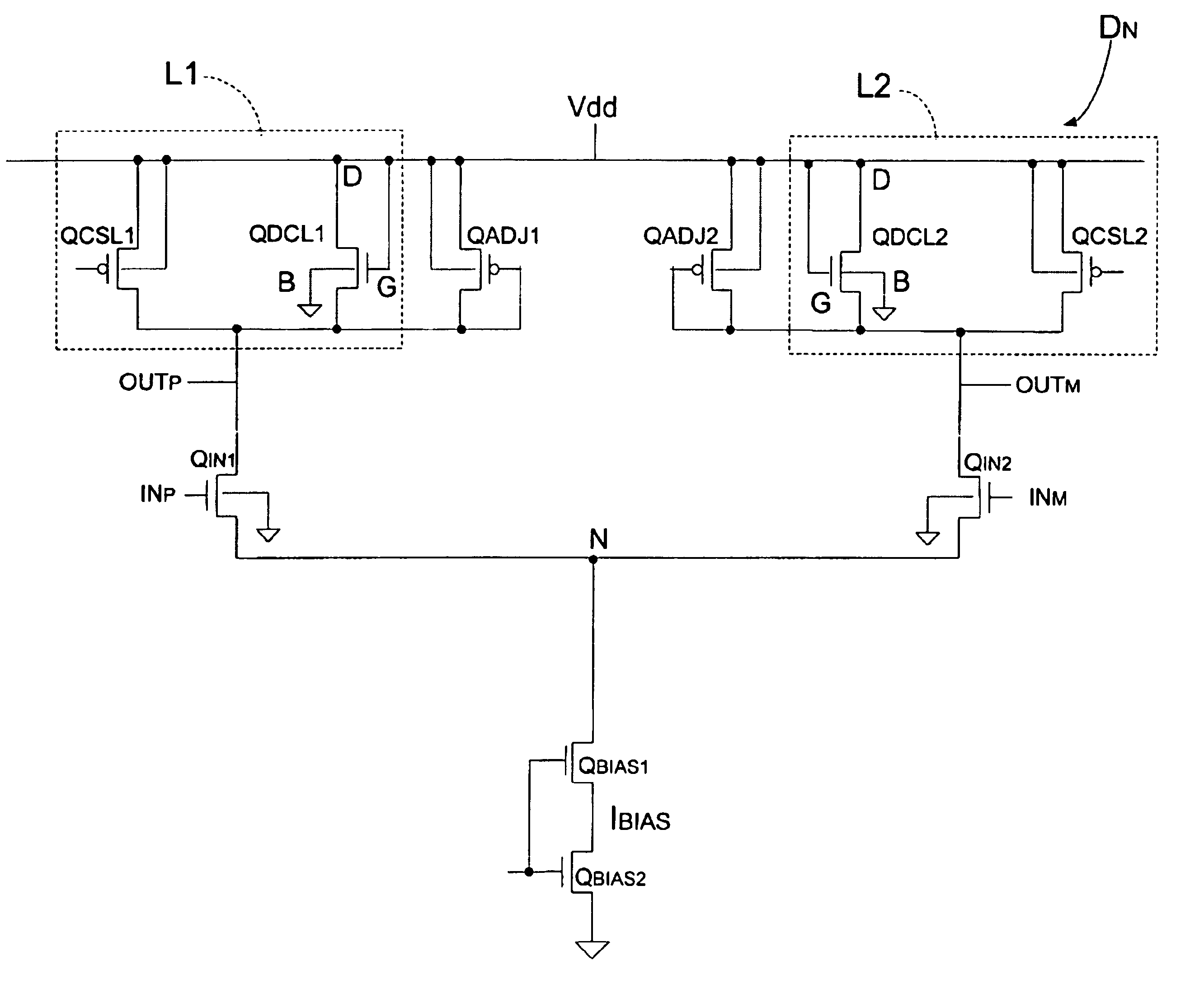
[0019]The delay cell of the present invention provides a low delay solution for high performance CMOS timing generators. This is accomplished by employing a negative feedback circuit at the load, thereby compensating the delay cell bias current and the output capacitance for any changes in VDD caused by noise. By minimizing the effects of a changing VDD, changes to the delay characteristics of the cell are also correspondingly minimized.

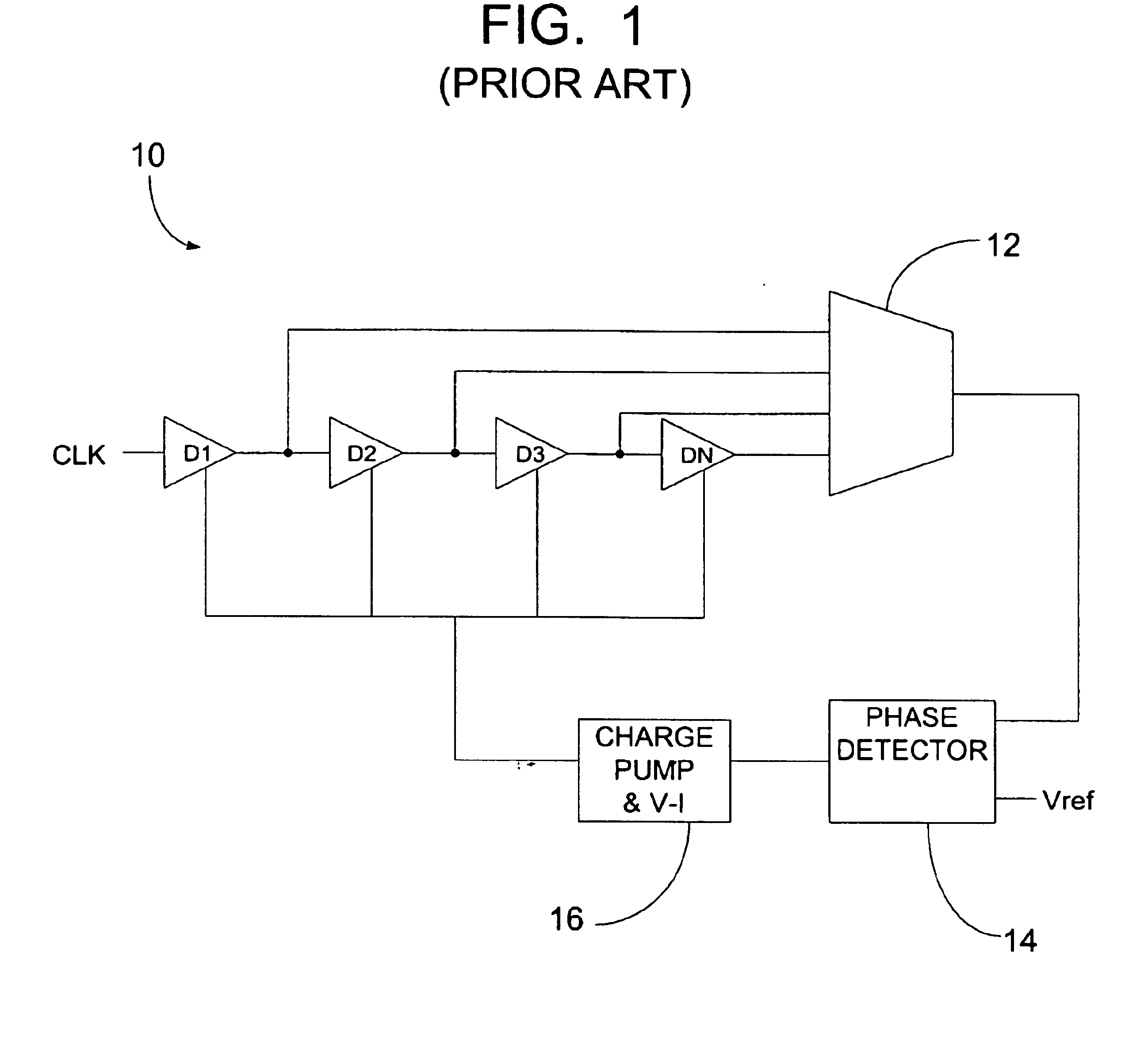
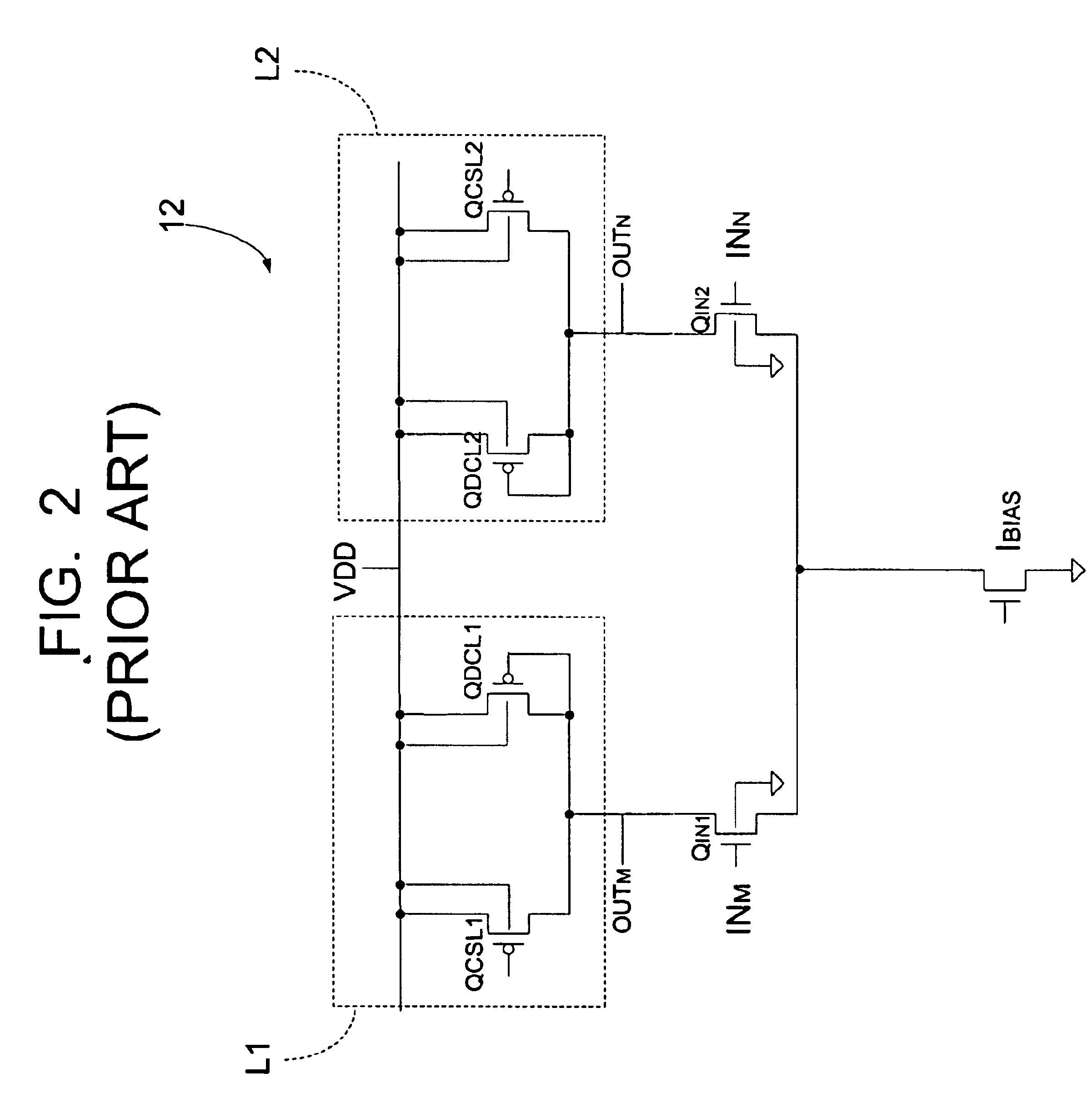
[0020]Referring now to FIG. 3, a timing generator according to one form of the present invention, generally designated 20, is shown for use with automatic test equipment. The timing generator is of the type that provides bias current compensation to control delay. The generator includes a delay line 22 comprising a set of N delay elements D1-DN, each providing a proportional to 1 / N phase offset with respect to an input clock CLK. The delay line is split into groups, such that the delay element outputs from one group are fed to a first multiplexer M1,...


PUM


Abstract

A differential delay cell is disclosed. The delay cell includes a voltage bus and a differential pair of MOS transistors having respective source terminals coupled to define a current node, and respective drain terminal outputs that cooperate to form a differential output. A current source is disposed at the current node while a differential diode-connected load is disposed between the differential pair and the voltage bus. The differential diode-connected load comprises at least one n-channel MOS transistor configured as a diode.

Description

FIELD OF THE INVENTION[0001]The invention relates generally to automatic test equipment, and more particularly low jitter timing generation circuits for automatic test equipment applications.BACKGROUND OF THE INVENTION[0002]Timing edge placement is often a critical parameter for high performance semiconductor testers. Having the ability to place the rising and / or falling edge of a test signal within a few picoseconds of a desired point in time may mean the difference in passing or failing large numbers of semiconductor devices under test.[0003]Conventional timing generators that produce high accuracy timing signals are often employed in CMOS integrated circuits. CMOS technology provides relatively good performance at very low cost. However, CMOS ICs are often susceptible to temperature and other conditions that affect the performance of the circuit. To counter this, many CMOS timing generators employ sophisticated compensation techniques to minimize changes in delay.[0004]With refer...

Claims


Application Information

Patent Timeline
IPC IPC(8): H03H11/26
CPCH03H11/265
Inventor IORGA, COSMINHUSSEY, ALANLING, KUOK
Owner TERADYNE
Why Eureka
Try Eureka