
Diffraction grating, method of making and method of using

Inactive Publication Date: 2005-05-17
DELPHI TECH INC
View PDF9 Cites 17 Cited by
  • Summary
  • Abstract
  • Description
  • Claims
  • Application Information

AI Technical Summary

Benefits of technology

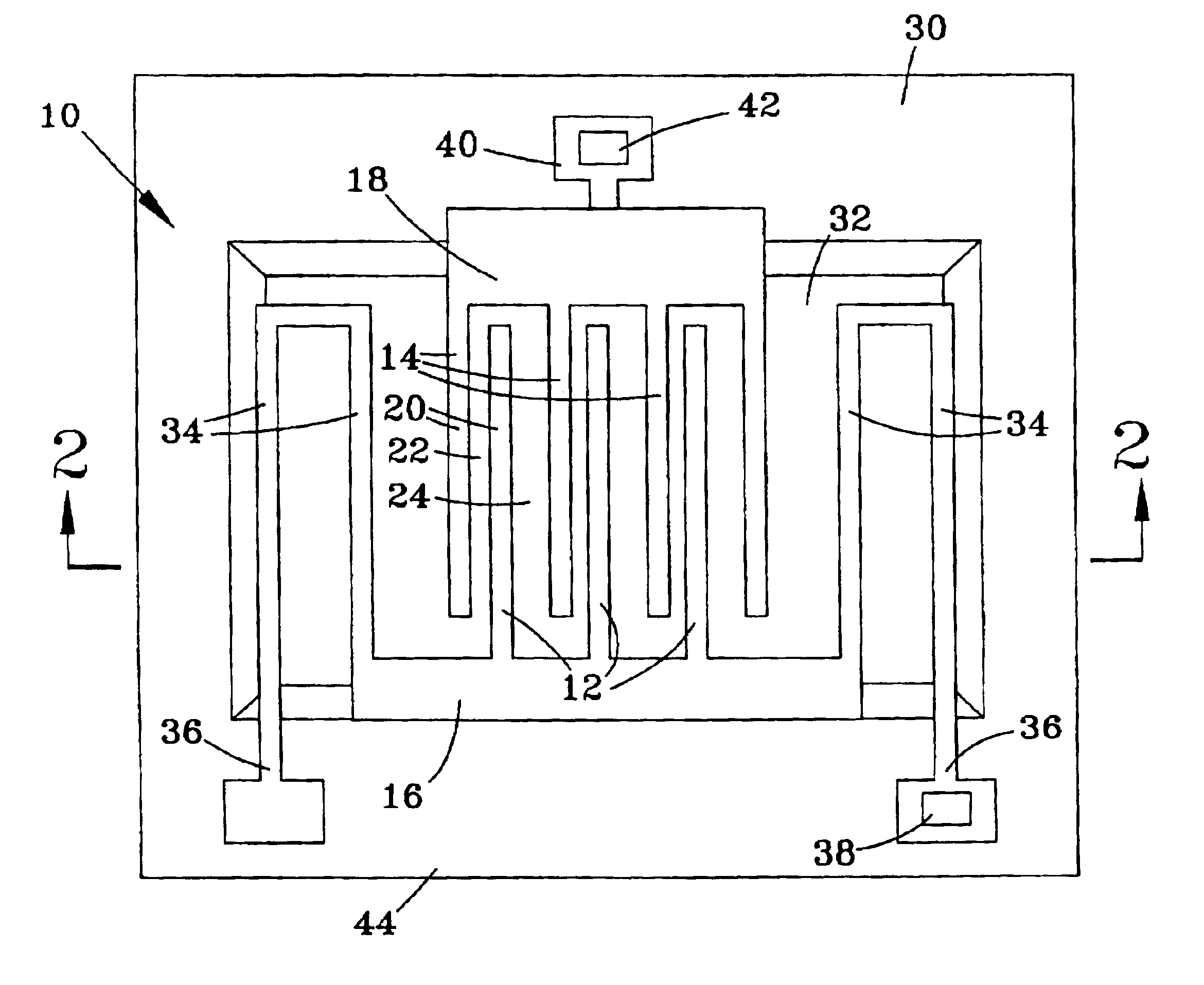
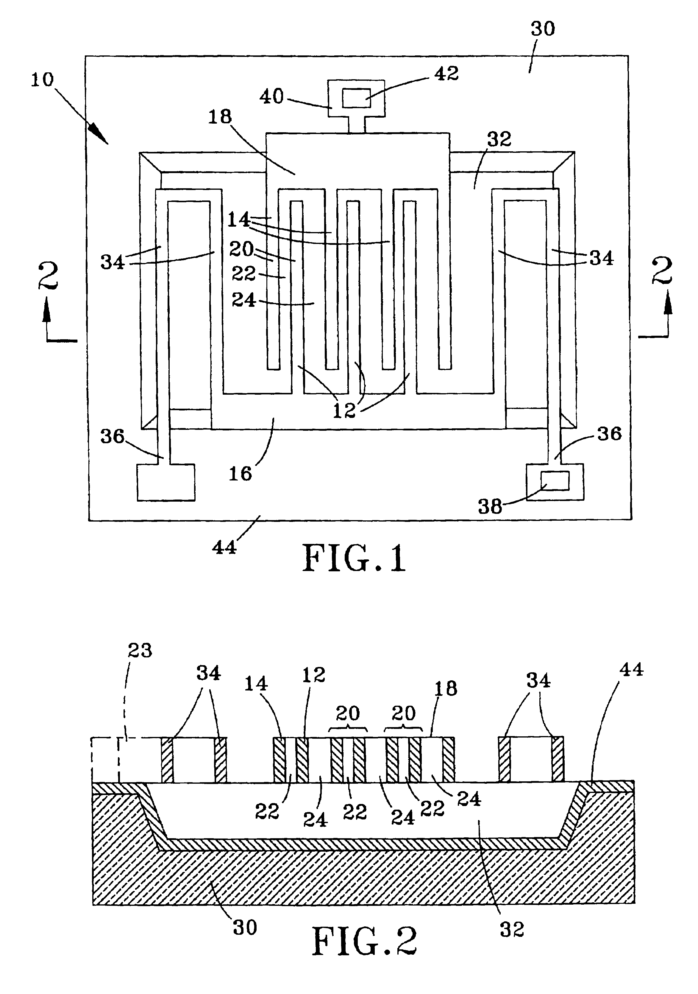
[0009]The present invention is a diffraction grating device and a method of manufacturing and using any number of such grating devices so that each device is individually electrically addressable to diffract radiation of different wavelengths, while also being configured to minimize device size, have minimal inactive (dark) areas, and have an uncomplicated addressing scheme. An example of an application for diffraction grating devices of this invention is a compact, reconfigurable full-color image source, in which each pixel is defined by a grating device. Such an image source can have a high pixel density as a result of reduced pixel size, minimal dark space per pixel, and a simplified addressing scheme. In addition to size and simplicity, diffraction grating devices of this invention also satisfy the current need for reconfigurable optical devices because of their ease of manufacture and utility.
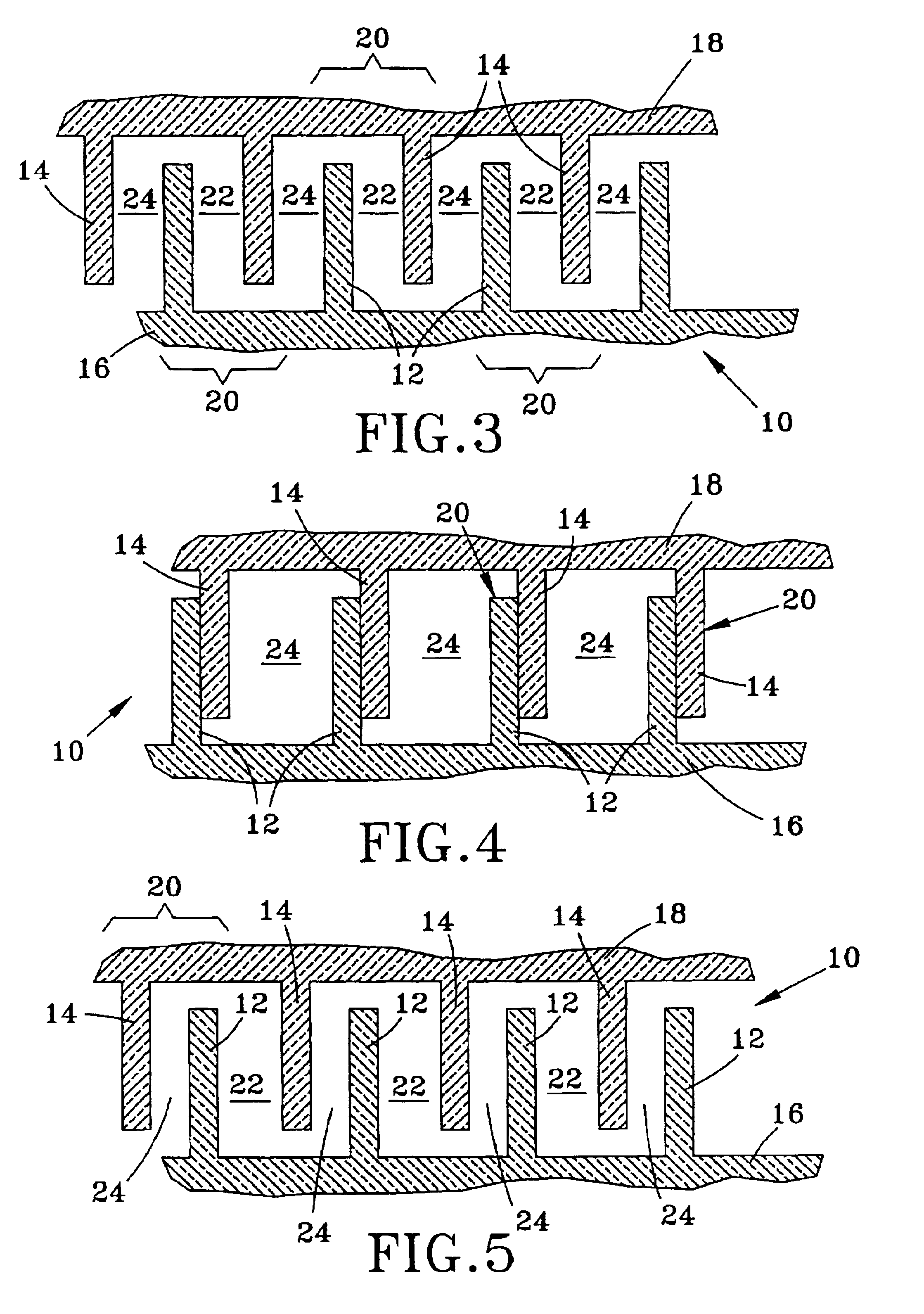
[0011]In view of the above, the gaps between the interdigitated elements of the invention are not fixed as in prior art diffraction gratings. Instead, the interdigitated elements are movable in-plane toward and away from each other, so that particular wavelengths are diffracted by controlling the gaps within and between the element pairs. The elements are individually electrically addressable to diffract radiation of any desired wavelength by precisely adjusting the gap widths, such as by capacitively charging the elements with a digital or analog signal. Any number of element pairs can be readily fabricated in a single device to achieve a small grating size with desirable dispersion and resolution levels. The interdigitated elements are configured so that each set of element pairs is capable of being electrically addressed in an uncomplicated manner. The result is a diffraction grating of minimal size, having minimal dark areas, and capable of precisely diffracting radiation of essentially any desired wavelength. When diffraction grating devices of this invention are used as pixels, an image source utilizing the devices is capable of having a high pixel density while retaining the ability to selectively diffract any chosen color, which are desirable characteristics of a full-color, reconfigurable image source such as a head-up display (HUD) for an automobile.

Problems solved by technology

A disadvantage of pixels formed of multiple gratings is that they are necessarily larger than pixels containing only one grating.
Another disadvantage is that any grating not being used to produce a specific color diffraction will be a dark space in the pixel.
Additionally, a difficulty arises because each grating in the pixel must be addressable so that the desired color for that pixel can be attained.
While addressing a grating can be easily accomplished using top side metal runners, at least two runner per grating is needed, each of which creates an undesirable dark space on the pixel.
As the number of gratings per pixel is increased to enhance the full color effect, a greater number of runners is likewise required, such that an array of such pixels becomes more complex and difficult to address, and pixel density is decreased resulting in a lower resolution for the pixel array.

Method used


Image

  • Diffraction grating, method of making and method of using
  • Diffraction grating, method of making and method of using
  • Diffraction grating, method of making and method of using

Examples


Embodiment Construction

[0021]The Figures represent various different embodiments and applications for a diffraction grating device in accordance with the present invention. In each case, the device can be adapted to operate as a reflection grating in which radiation is diffracted by reflection, or as a transmission grating in which radiation is diffracted by transmission through gaps. Any number of these devices can be used in various optical devices, including optical switches, chromatographs, and reconfigurable full-color image sources. In the latter, each grating device is an individually and electrically addressable pixel of the image source. The small grating size and simple addressing schemes made possible with this invention enable the individual pixels to be small with minimal dark spaces, thus enabling the image source to have a high pixel density and a high level of resolution. While the following discussion will focus on diffracting spectral light to produce visible light of desired colors, tho...


PUM


Abstract

A diffraction grating device operable as a reflection or transmission grating, and a method of manufacturing and using any number of such grating devices so that each device is individually electrically addressable to diffract radiation of different wavelengths. The grating device comprises first and second sets of interdigitated elements so that each element of the first set defines an element pair with an immediately adjacent element of the second set, a first gap is defined between the elements of each element pair, and a second gap is defined between each adjacent pair of element pairs. The elements of an element pair are selectively movable toward and away from each other. As such, the widths of the gaps can be selectively sized to diffract radiation of a desired wavelength.

Description

CROSS REFERENCE TO RELATED APPLICATIONS[0001]Not applicable.STATEMENT REGARDING FEDERALLY-SPONSORED RESEARCH[0002]Not applicable.BACKGROUND OF THE INVENTION[0003](1) Field of the Invention[0004]The present invention generally relates to methods and devices for modulating radiation, such as when a light beam is modulated to produce a color image. More particularly, this invention relates to a diffraction grating device with interdigitized elements that can be individually electrically addressable to diffract radiation of different wavelengths, and can be used in a variety of optical devices, such as a compact, reconfigurable full-color image source.[0005](2) Description of the Related Art[0006]Devices with individual electrically-addressable elements have been considered for use in full-color, reconfigurable image sources, such as head-up displays (HUD's) in automobiles. Such devices generally provide a full color image source by modulating a light beam with the use of numerous pixel...

Claims


Application Information

Patent Timeline
IPC IPC(8): G02B26/08
CPCG02B26/0808
Inventor CHRISTENSON, JOHN C.
Owner DELPHI TECH INC
Learn More