CTE compensation of semiconductor laser bars

a laser bar and semiconductor technology, applied in semiconductor lasers, manufacturing tools, soldering apparatus, etc., can solve the problems of premature failure at high power output, shorten the useful life, and reduce the surface area available for heat transfer, so as to limit the useful life of laser bars

Inactive Publication Date: 2005-05-17
SPECTRA PHYSICS SEMICON LASERS
View PDF7 Cites 22 Cited by
  • Summary
  • Abstract
  • Description
  • Claims
  • Application Information

AI Technical Summary

Benefits of technology

[0003]In accordance with the principles of the invention, in one illustrative embodiment, the CTE of a conventional microchannel copper heat sink is locally modified in the area where the laser bar is soldered. A strip of ceramic material having a CTE lower than that of the laser bar and the copper heat sink is soldered to portions of the metallic heat sink located adjacently to the surface area on which the laser bar is located. The inclusion of the ceramic strips enable a laser bar having a nominal CTE of 6.6×10⁻⁶ / K, to be soldered directly to a copper heat sink having a nominal CTE of 16.5×10⁻⁶ / K without incurring thermal distortions at the interface that limit the useful life of the laser bar.

Problems solved by technology

Warpage of the substrate reduces the surface area available for heat transfer.
Despite such approaches, premature failures still occur at high power outputs, especially in laser bars subjected to pulsed operation where alternate heating and cooling can shorten the useful life (generally defined as a 20% reduction in useful output power) from 10,000 hours to only 1000 hours.

Method used


Image

  • CTE compensation of semiconductor laser bars
  • CTE compensation of semiconductor laser bars
  • CTE compensation of semiconductor laser bars

Examples


Embodiment Construction

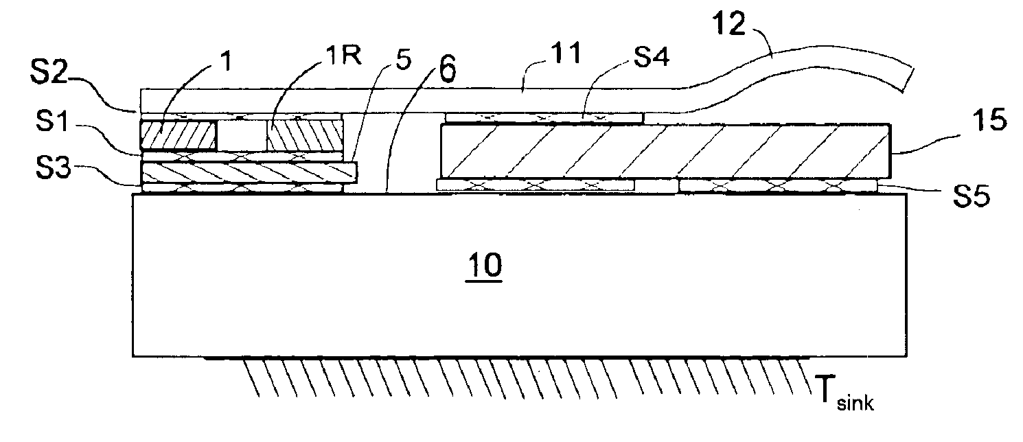
[0010]Referring to FIG. 1 the prior art method of mounting a laser bar 1 to a heat sink 10, such as that shown in U.S. Pat. No. 6,272,159, requires the use of a ceramic submount 5 whose CTE matches that of the laser bar. The use of a submount 5 requires two solder joints S1 and S3 in addition to the solder joint between laser bar 1 and spring contact 11. Each of the solder joints will have a thickness that depends on the type of solder used and the materials being joined. Illustratively, joint S1 between laser bar 1 and ceramic substrate 5 is a 25μ thick Au—Sn “preform” solder joint; joint S2 Between laser bar 1 and spring contact 11 is a 25μ thick InAg solder joint; joint S3 between ceramic substrate 5 and heat sink 10 is a 37μ thick In solder preform joint. A surge protecting reverse diode 1R, as described in U.S. Pat. No. 6,028,878 assigned to the assignee of the present invention, may also be soldered in tandem with laser bar 1. Electrical contact to laser diode bar 1 is provide...


PUM

PropertyMeasurementUnit
lengthaaaaaaaaaa
coefficients of thermal expansionaaaaaaaaaa
coefficient of thermal expansionaaaaaaaaaa

Abstract

A laser bar is soldered to a conventional microchannel copper heat sink whose coefficient of thermal expansion (CTE) is locally modified in the area where the laser bar is soldered to better match the CTE of the laser bar. A strip of ceramic material having a CTE lower than that each of the laser bar and of the copper heat sink is soldered to portions of the metallic heat sink located adjacently to the surface area on which the laser bar is located. The inclusion of the ceramic strips enables a laser bar having a nominal CTE of 6.6×10⁻⁶/K, to be soldered directly to a copper heat sink having a nominal CTE of 16.5×10⁻⁶/K without incurring thermal distortions at the interface that would limit the useful life of the laser bar.

Description

FIELD OF THE INVENTION[0001]This invention relates to high power laser bars and, more particularly, to extending their useful life.BACKGROUND OF THE PRIOR ART[0002]High power laser diode bars are commercially available in a variety of configurations including vertical and horizontal stacks such as shown in U.S. Pat. No. 6,272,159. Because the heat generated in a laser bar must be effectively dissipated, it is important that the thermal resistance at the laser bar's interface with the heat sink be low and that an efficient heat sink, such as a microchannel heat sink, constructed of thin copper plates between which water is pumped, be used. A micro-channel heat sink is shown in U.S. Pat. No. 6,268,653. In addition to low thermal resistance at the interface it is important that the materials as the interface have closely related coefficients of thermal expansion to avoid the influence of stress in thermal cycling. The '653 patent suggested that thermal stress from high temperature sold...

Claims


Application Information

Patent Timeline
Patent Type & Authority Patents(United States)
IPC IPC(8): B23K1/00B23K33/00H01S5/40H01S5/00H01S5/02H01S5/024
CPCB23K1/0008B23K33/00B23K33/008H01S5/4025B23K2201/02H01S5/02272H01S5/02423B23K2201/006B23K2101/006B23K2101/02H01S5/0237
Inventor TREUSCH, HANS-GEORGBONATI, GUIDO
Owner SPECTRA PHYSICS SEMICON LASERS
Why Eureka
Try Eureka