Generation of pulse signals from a clock signal

a clock signal and pulse signal technology, applied in the direction of generating/distributing signals, pulse techniques, instruments, etc., can solve the problems of large errors, low cycle duration of clock signals, and disadvantages of conventional pulse signal generating circuits, so as to minimize the effect of delay values and reduce delay values

Inactive Publication Date: 2005-05-17
SEIKO EPSON CORP
View PDF6 Cites 6 Cited by
  • Summary
  • Abstract
  • Description
  • Claims
  • Application Information

AI Technical Summary

Benefits of technology

[0019]In the pulse signal generating circuit, the effect of variations in the delay value is less than that observed when a pulse signal is generated from only the rising edges of a clock signal. As a result, it is possible to satisfy the required values for specific periods of pulse signals without an undue reduction in the cycle duration of a clock signal, even taking into account variations in the delay value of delay circuits.
[0020]The cycle duration of a pulse signal is preferably set equal to the cycle duration of the clock signal. Adopting this approach makes it possible to minimize the effect of variations in delay va...

Problems solved by technology

In this circuit design, fairly large errors are envisaged for the delay times Td1 and Td2 under consideration for the nonuniformity of delay times due to manufacturing errors, and temperature dependence.
A conventional pulse signal generating circ...

Method used


Image

  • Generation of pulse signals from a clock signal
  • Generation of pulse signals from a clock signal
  • Generation of pulse signals from a clock signal

Examples


second embodiment

B. Second Embodiment

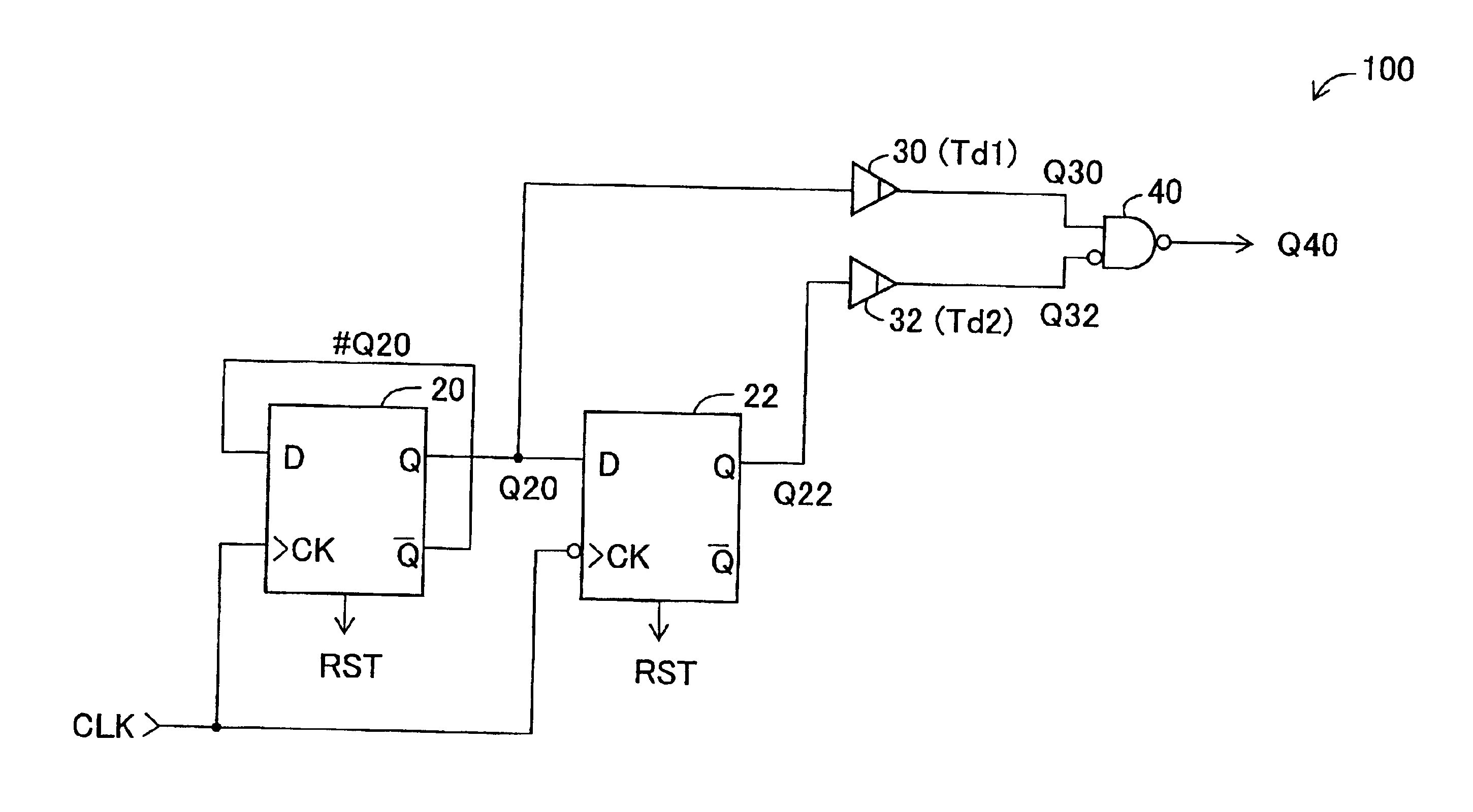
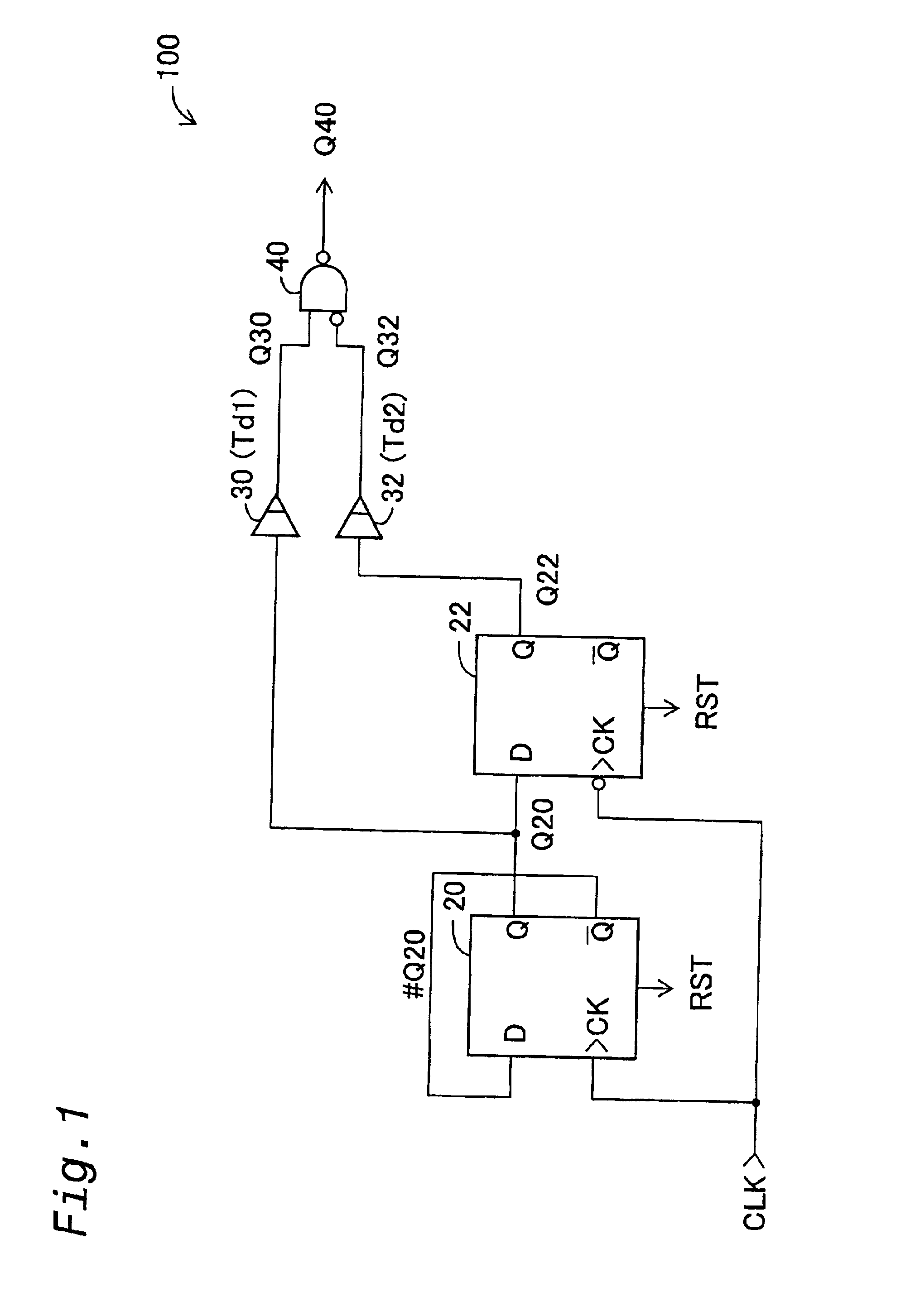
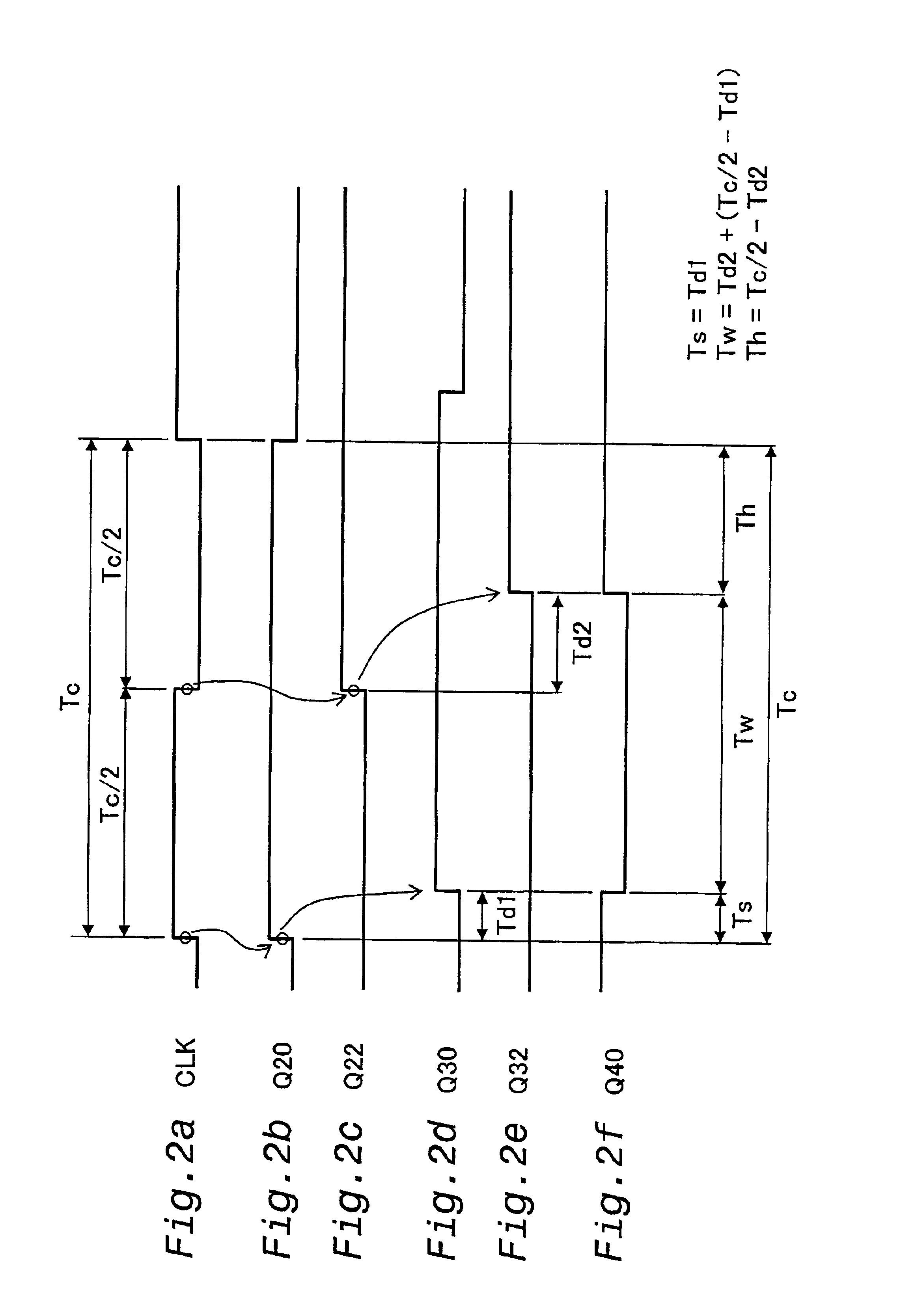
[0079]FIG. 7 is a block diagram depicting the structure of a pulse signal generating circuit 110 as a second embodiment of the present invention. The circuit 110 comprises a first-stage circuit 112, a second-stage circuit 114, and an AND gate 50. The first-stage circuit 112 has the same structure as the pulse signal generating circuit 100 of the first embodiment shown in FIG. 1. The second-stage circuit 114 comprises two DFFs 24 and 26, two delay circuits 34 and 36, and a NAND gate 42 in which one of the two input terminals is an inverted input terminal. The connections between the elements of the second-stage circuit 114 are substantially the same as the connections between the elements of the first-stage circuit 112. The delay circuits 34 and 36 in the second-stage circuit 114 have the same delay times Td1 and Td2 as the delay circuits 30 and 32 in the first-stage circuit 112. The D input terminal of the first DFF 24 in the second-stage circuit 114 is supplied ...

third embodiment

C. Third Embodiment

[0083]FIG. 9 is a block diagram depicting a pulse signal generating circuit 120 pertaining to a third embodiment of the present invention. The pulse signal generating circuit 120 is obtained by removing the two DFFs 24 and 26 from the circuit of the second embodiment shown in FIG. 7. Another feature of the circuit 120 is that the inputs of the delay circuits 34 and 36 are different from those of the circuit pertaining to the second embodiment. Specifically, the inverted output of the first DFF 20 is provided to a delay circuit 34 having a first delay time Td1, and the inverted output of the second DFF 22 is provided to a delay circuit 36 having a second delay time Td2.

[0084]The pulse signal generating circuit 120 of the third embodiment can generate substantially the same pulse signal Sout as the pulse signal generating circuit 110 of the second embodiment. Another advantage of the third embodiment is that its circuit structure is simpler than that of the second e...

fourth embodiment

D. Fourth Embodiment

[0085]FIG. 10 is a block diagram depicting the structure of a pulse signal generating circuit 130 pertaining to a fourth embodiment of the present invention. The structure of the pulse signal generating circuit 130 is obtained by removing the two delay circuits 34 and 36 from the circuit of the third embodiment shown in FIG. 9. Another feature of the pulse signal generating circuit 130 is that the output Q30 of the first delay circuit 30 is provided to the noninverted input terminal of a first NAND gate 40 and the inverted input terminal of a second NAND gate 42. The output Q32 of the second delay circuit 32 is provided to the inverted input terminal of the first NAND gate 40 and the noninverted input terminal of the second NAND gate 42.

[0086]The pulse signal generating circuit 130 of the fourth embodiment can generate substantially the same pulse signal Sout as the one generated by the pulse signal generating circuit of the second or third embodiment. Another ad...


PUM


Abstract

Two first delay signals Q30 and Q34 are generated such that edges thereof are delayed by a first delay time Td1 in relation to the rising edge of a clock signal CLK. Two second delay signals Q32 and Q36 are also generated such that edges thereof are delayed by a second delay time Td2 in relation to the trailing edge of the clock signal CLK. A pulse signal Sout is generated as a result of logic operations performed on the first delay signals Q30 and Q34 and the second delayed signals Q32 and Q36.

Description

BACKGROUND OF THE INVENTION[0001]1. Field of the Invention[0002]The present invention relates to a technique for generating a specific pulse signal from a clock signal having a fixed cycle.[0003]2. Description of the Related Art[0004]FIG. 13 is a block diagram depicting a conventional pulse signal generating circuit 200 for generating a specific pulse signal Q230 from a clock signal CLK. The circuit 200 comprises a D flip-flop 210 (henceforth referred to as “DFF 210”), two delay circuits 220 and 222 connected in series, and a NAND gate 230 in which one of the two input terminals is an inverted input terminal. The clock signal CLK is supplied to the clock input terminal of the DFF 210. The output Q210 of the DFF 210 is supplied to the first delay circuit 220, and the inverted output #Q210 is fed back to its D input terminal. The delay signal Q220 delayed by the first delay circuit 220 is supplied to the noninverted input terminal of the NAND gate 230. The delay signal Q220 is also su...

Claims


Application Information

Patent Timeline
IPC IPC(8): G06F1/12H03K3/86H03K5/135H03K3/00H03L7/00H03K5/14H03K5/13
CPCH03K5/135H03K5/131
Inventor OTSUKA, SYUJI
Owner SEIKO EPSON CORP
Why Eureka
Try Eureka