Integrated circuit with reverse engineering protection

a reverse engineering protection and integrated circuit technology, applied in semiconductor devices, semiconductor/solid-state device details, electrical apparatus, etc., can solve the problems of reverse engineering being unable to use automatic circuit and pattern recognition techniques in order to reverse engineer an integrated circuit, and the creation of complex integrated circuits and semiconductor devices can be a very expensive undertaking

Inactive Publication Date: 2005-05-24
RAYTHEON CO
View PDF142 Cites 26 Cited by
  • Summary
  • Abstract
  • Description
  • Claims
  • Application Information

AI Technical Summary

Benefits of technology

[0008]In order to keep the reverse engineer at bay, different techniques are known in the art to make integrated circuits more difficult to reverse engineer. One technique is to make the connections between transistors difficult to determine forcing the reverse engineer to carefully analyze each transistor (in particular each CMOS transistor pair for CMOS devices). Bit camouflaging the connections between transistors, the reverse engineer is unable to use automatic circuit and pattern recognition techniques in order to reverse engineer an integrated circuit. Since integrated circuits can have hundreds of thousands or even millions of transistors, forcing the reverse engineer to carefully analyze each transistor in a device can effectively frustrate the reverse engineer's ability to reverse engineer the device successfully.
[0010]It is an object of this invention to make reverse engineering even more difficult and, in particular, to force the reverse engineer to study the possible silicon-to-gate poly lines very carefully, to see if they are in fact real. It is believed that this will make the reverse engineer's efforts all the more difficult by making it very time consuming in order to reverse engineer a chip employing the present invention and perhaps making it exceedingly impractical, if not impossible, to reverse engineer a chip employing the present invention.
[0018]Another aspect of the present invention provides a method of deterring a reverse engineer comprising the steps of: associating at least one conductive contact with an active area; and preventing electrical conduction between said at least one conductive contact and said active area by inserting an intervening insulating layer.
[0022]Another aspect of the present invention provides a method for confusing a reverse engineer comprising the steps of: implanting an active region in a substrate; associating a conductive layer with said active region; disposing at a dielectric layer over said conductive layer; and providing a control electrode, wherein said dielectric layer prevents said conductive layer from influencing conduction through said active region in response to an application of control voltages to said control electrode.

Problems solved by technology

The creation of complex integrated circuits and semiconductor devices can be a very expensive undertaking given the large number of hours of sophisticated engineering talent involved in designing such devices.
One technique is to make the connections between transistors difficult to determine forcing the reverse engineer to carefully analyze each transistor (in particular each CMOS transistor pair for CMOS devices).
Bit camouflaging the connections between transistors, the reverse engineer is unable to use automatic circuit and pattern recognition techniques in order to reverse engineer an integrated circuit.
Since integrated circuits can have hundreds of thousands or even millions of transistors, forcing the reverse engineer to carefully analyze each transistor in a device can effectively frustrate the reverse engineer's ability to reverse engineer the device successfully.
It is believed that this will make the reverse engineer's efforts all the more difficult by making it very time consuming in order to reverse engineer a chip employing the present invention and perhaps making it exceedingly impractical, if not impossible, to reverse engineer a chip employing the present invention.

Method used


Image

  • Integrated circuit with reverse engineering protection
  • Integrated circuit with reverse engineering protection
  • Integrated circuit with reverse engineering protection

Examples


Embodiment Construction

relating to the camouflage of integrated circuit devices in order to make it more difficult to reverse engineer them as discussed above. The present invention can often be used harmoniously with the techniques disclosed in these prior United States Patents to further confuse the reverse engineer.

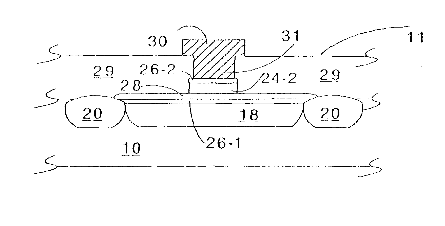
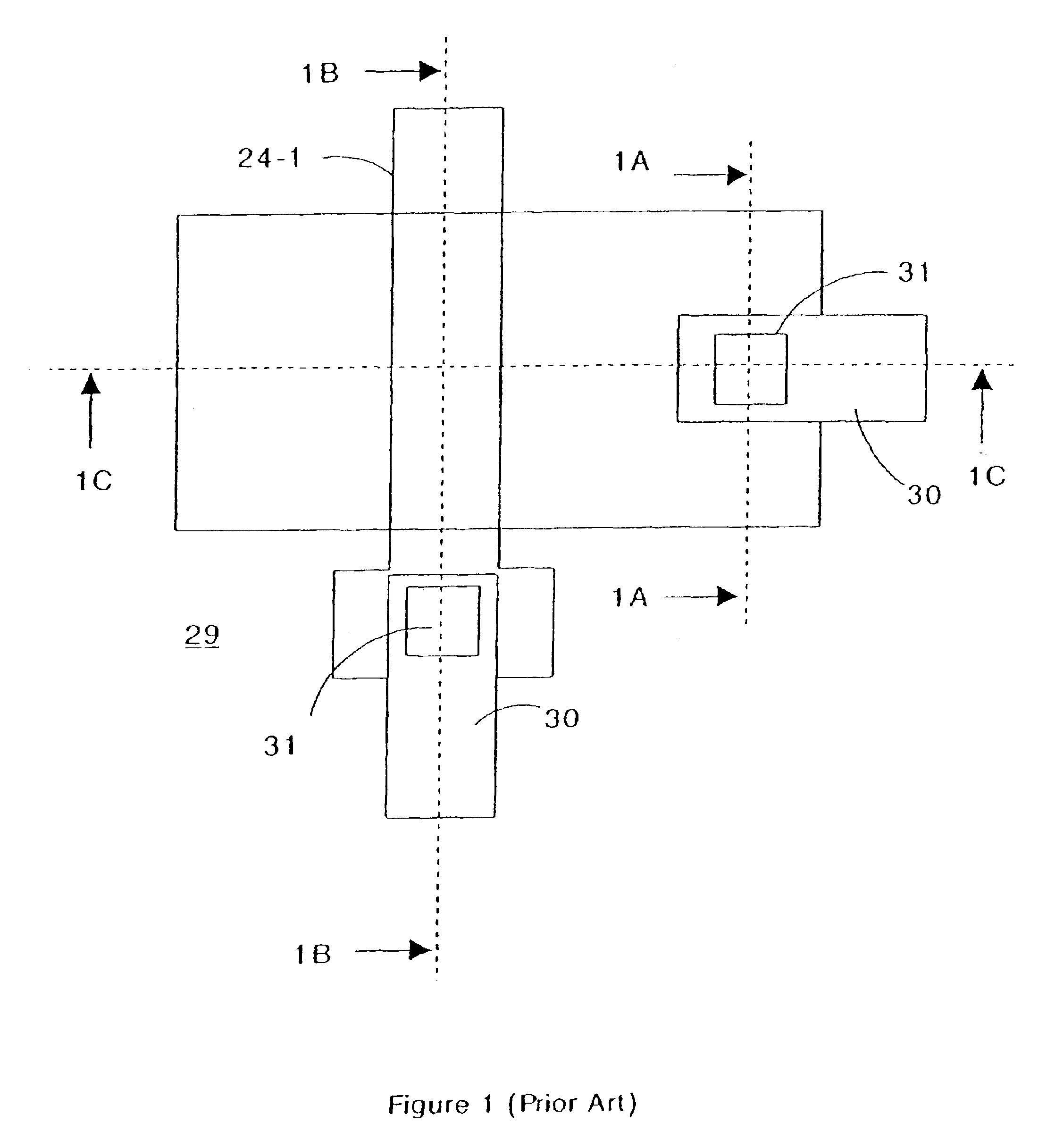
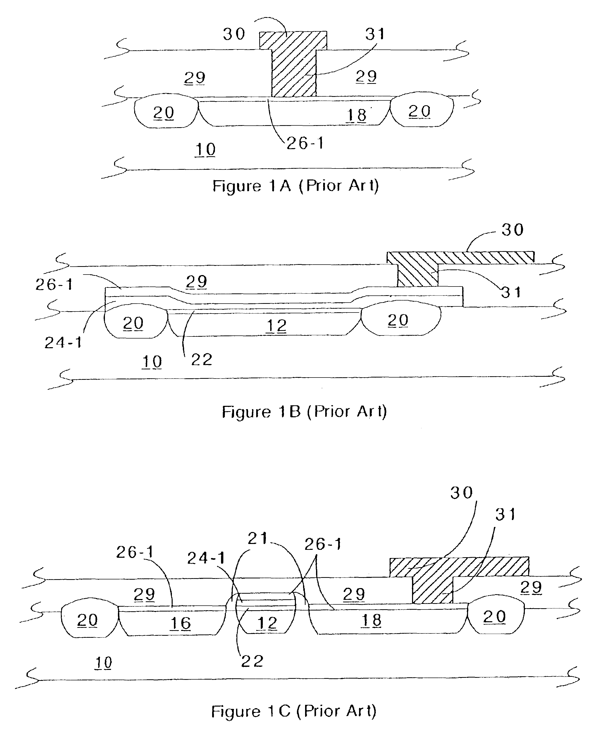
[0012]In modern semiconductor manufacturing processes, particularly where the feature size is less than 0.5 micrometers, a silicide layer is typically used to improve conductivity. FIG. 1 is a plan view of a semiconductor device. FIGS. 1A, 1B and 1C are cross-sectional views of the semiconductor device shown in plan view in FIG. 1. A typical drain or source contact is shown in FIG. 1A, while a typical gate contact is shown in FIG. 1B. The drain, source and gate regions are formed on a semiconductor substrate, such as silicon substrate 10, and have active regions 12, 16, 18, as shown in FIG. 1C, formed therein, typically by implantation of a suitable dopant. Field oxide (FOX) 20 is used to he...


PUM


Abstract

Technique and structures for camouflaging an integrated circuit structure. The integrated circuit structure is formed by a plurality of layers of material having controlled outlines and controlled thicknesses. A layer of dielectric material of a controlled thickness is disposed among said plurality of layers to thereby render the integrated circuit structure intentionally inoperable.

Description

CROSS REFERENCE TO RELATED APPLICATIONS[0001]This application claims the benefit of U.S. Provisional Patent Application 60 / 378,155 filed May 14, 2002, which application is incorporated herein by reference.TECHNICAL FIELD[0002]The present invention relates to integrated circuits and semiconductor devices (ICs) in general and their methods of manufacture wherein the integrated circuits and semiconductor devices employ camouflaging techniques which make it difficult for a reverse engineer to discern how the semiconductor device is manufactured.RELATED ART[0003]The present invention is related to the following U.S. Patents, all of which were filed by the same inventors:[0004](1) U.S. Pat. Nos. 5,866,933; 5,973,375 and 6,294,816 teach how transistors in a CMOS circuit are connected by implanted (and therefore hidden and buried) lines between the transistors by modifying the p+ and n+ source / drain masks. These implanted interconnections are used to make 3-input AND and 3-input OR circuits...

Claims


Application Information

Patent Timeline
Patent Type & Authority Patents(United States)
IPC IPC(8): H01L23/58H01L27/02
CPCH01L23/573H01L27/0203H01L27/02H01L2924/0002H01L2924/00
Inventor CHOW, LAP-WAICLARK, JR., WILLIAM M.BAUKUS, JAMES P.
Owner RAYTHEON CO
Why Eureka
Try Eureka