
Memory bus polarity indicator system and method for reducing the affects of simultaneous switching outputs (SSO) on memory bus timing

a memory bus and polarity indicator technology, applied in the field of integrated circuits, can solve the problems of spurious data, shifts between dqs signal and data words becoming more critical, and undesirable skew or shift of read,

Inactive Publication Date: 2005-05-24
MICRON TECH INC
View PDF6 Cites 35 Cited by
  • Summary
  • Abstract
  • Description
  • Claims
  • Application Information

AI Technical Summary

Problems solved by technology

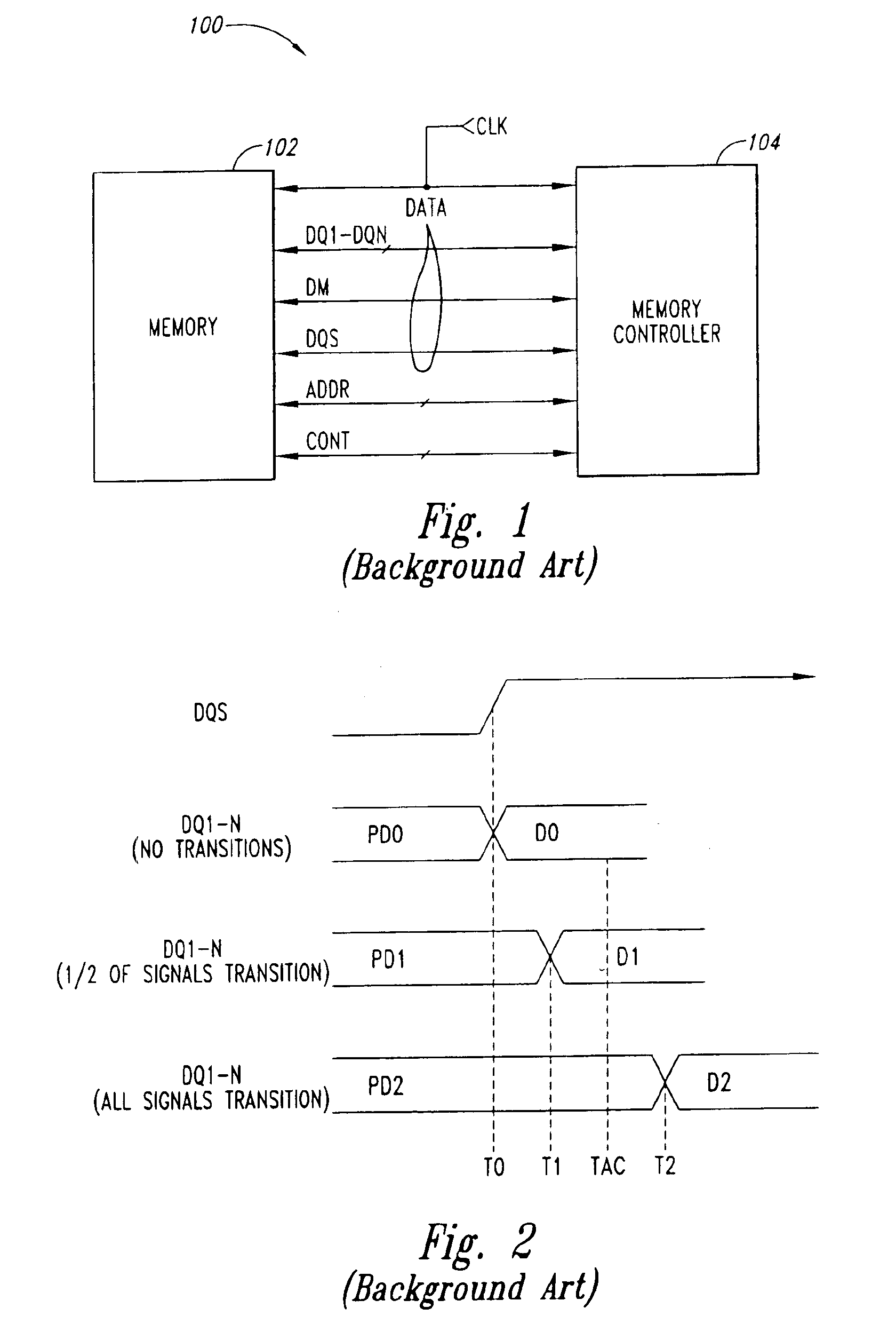
As a result, shifts between the DQS signal and the data words become more critical since a smaller shift may now result in spurious data being captured.
This increase in the width N of the data bus DATA can result in an undesirable skew or shift of the read data words DQ1-N relative to the DQS signal.
The reduced current causes the data drivers to drive the corresponding bits to the complementary logic states more slowly and thereby undesirable shifts the data word DQ1-N relative to the DQS signal, possibly shifting the data word outside the specified access time for the memory 102.
In addition to a reduced current being supplied to the data drivers, physical constraints on the size of the power lines (not shown) that supply power to the data drivers can result in the power lines having an inductance that causes a relatively large voltage drop to develop across the power lines when the data drivers demand a maximum current over a short period of time (V=Ldi / dt).
Such a voltage drop can also slow the rate at which the data drivers drive the corresponding bits to the required voltage levels and shift the data words outside the specified access time.
Additional power could be supplied to the data drivers to eliminate these undesirable shifts, but it is not always practicable or cost effective to increase the power, as will be appreciated by those skilled in the art.
This approach requires the inclusion of additional pins on the processor and receiving devices, which increases the cost of the processor and receiving devices due to the increased number of pins, as will be appreciated by those skilled in the art.
Moreover, as the width of the data bus increases, more DBI signals and associated pins are required, which consumes even more pins on the processor and receiving devices.

Method used


Image

  • Memory bus polarity indicator system and method for reducing the affects of simultaneous switching outputs (SSO) on memory bus timing
  • Memory bus polarity indicator system and method for reducing the affects of simultaneous switching outputs (SSO) on memory bus timing
  • Memory bus polarity indicator system and method for reducing the affects of simultaneous switching outputs (SSO) on memory bus timing

Examples


Embodiment Construction

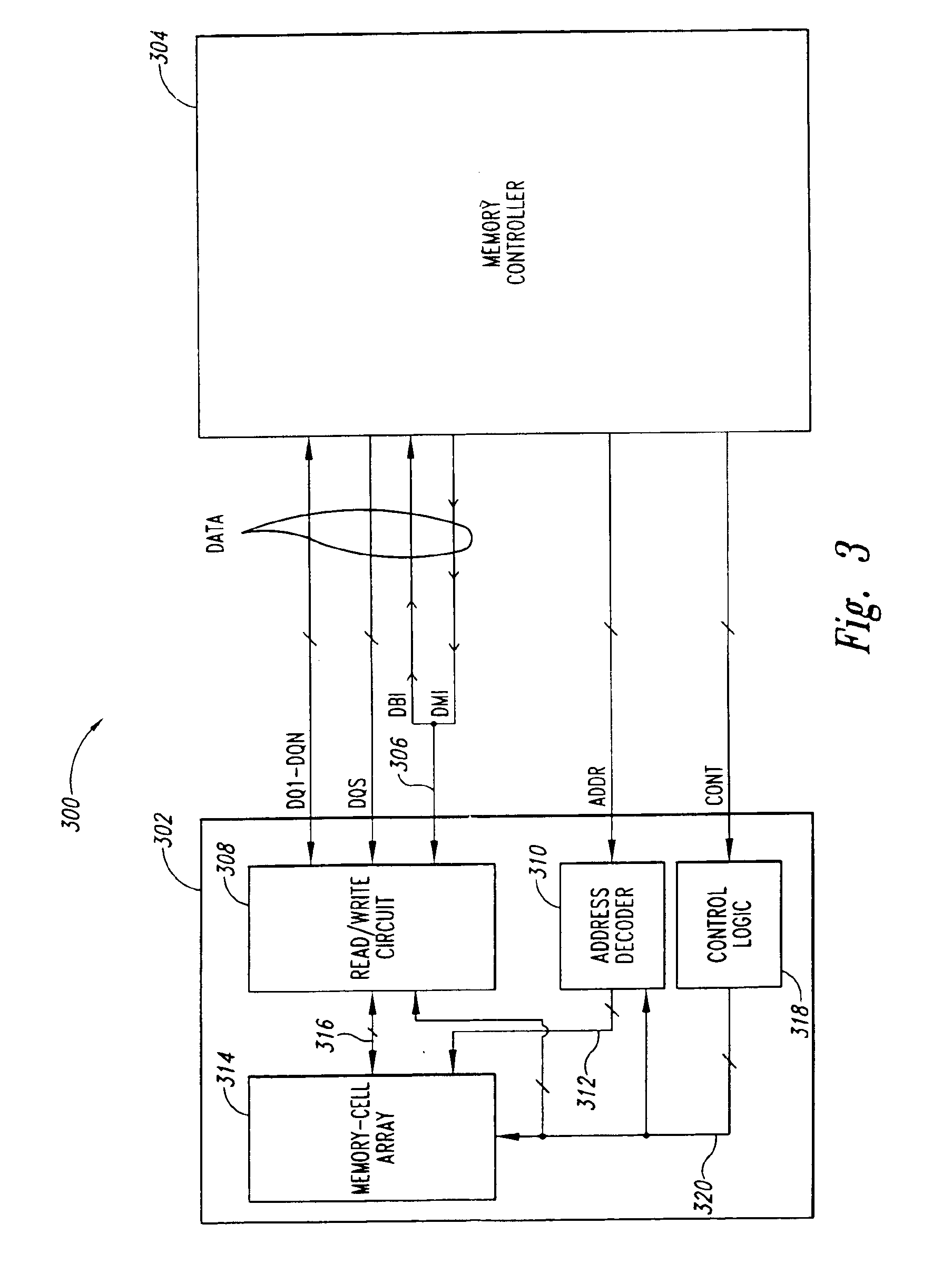
[0024]FIG. 3 is a functional block diagram illustrating a memory system 300 including a memory 302 that transfers data bus inversion information to a memory controller 304 over a data masking pin 306 of the memory during read data transfer operations. The memory 302 selectively outputs true or inverted read data words DQ1-N on a data bus DATA to minimize the switching of bits between consecutive read data words, and activates a data bus inversion signal DBI on the data masking pin 306 when inverted data is output and deactivates the DBI signal when true data is output, as will be explained in more detail below. The data masking pin 306 would normally be unused during read operations, but in the memory system 300 the memory 302 uses the data masking pin to apply the DBI signal to the memory controller 304 during read operations and in this way eliminates the need for additional dedicated pins on both the memory and memory controller, which reduces the costs of these devices. Moreover...


PUM


Abstract

A method and system transfer read data from a memory device having a data bus and a data masking pin adapted to receive a masking signal during write operations of the memory device. The method includes placing a sequence of read data words on the data bus and applying a data bus inversion signal on the data masking pin, the data bus inversion signal indicating whether the data contained each read data word has been inverted. Another method and system transfer data over a data bus. The method includes generating a sequence of data words, at least one data word including data bus inversion data. The sequence of data words is applied on the data bus and is thereafter stored. The data bus inversion data is applied to invert or not invert the data contained in the stored data words.

Description

TECHNICAL FIELD[0001]The present invention relates generally to integrated circuits, and more specifically to synchronizing a clock signal with data signals being transferred to and from an integrated circuit.BACKGROUND OF THE INVENTION[0002]In synchronous systems, devices in the system are clock clocked by an external clock signal and perform operations at predetermined times relative the rising and falling edges of the clock signal. For example, in a typical memory system, a memory controller applies commands to synchronous memory devices and data is transferred between the memory devices and the controller in synchronism with an external clock signal applied to the controller and memory devices. In the memory system, the memory controller must place write data being transferred to the memory devices on a data bus at the proper times relative to rising and falling edges of the external clock signal to ensure that the memory devices successfully capture the data. Similarly, the mem...

Claims


Application Information

Patent Timeline
IPC IPC(8): G06F13/42
CPCG06F13/4243
Inventor LABERGE, PAUL A.
Owner MICRON TECH INC
Learn More