

Timing-driven placement method utilizing novel interconnect delay model
a timing-driven placement and delay model technology, applied in computer aided design, program control, instruments, etc., can solve the problems of increasing the interconnect delay at critical nets, prone to many errors, and difficult to realize physical design without the aid of computers
- Summary
- Abstract
- Description
- Claims
- Application Information
AI Technical Summary
Benefits of technology
Problems solved by technology
Method used
Image


Examples
Embodiment Construction
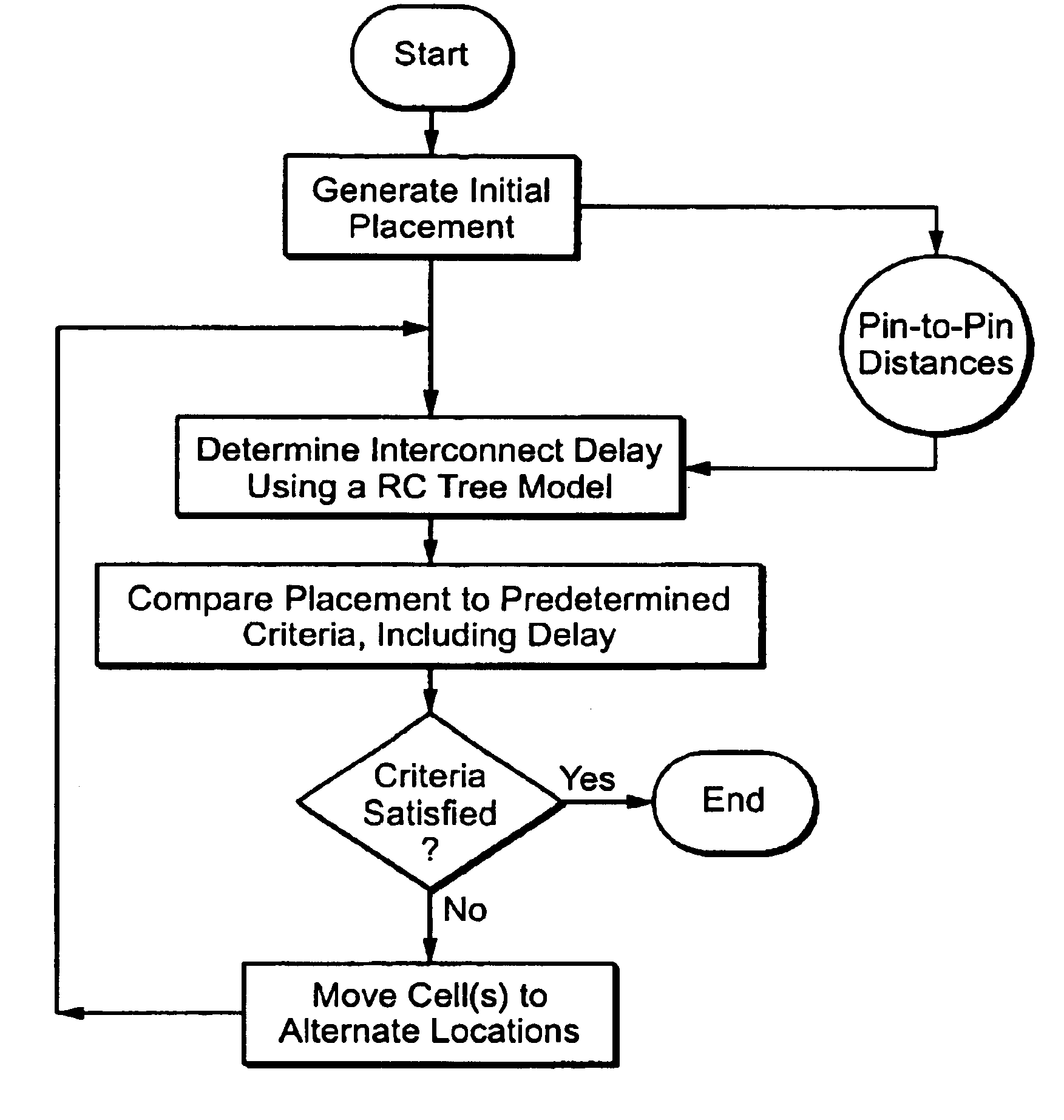
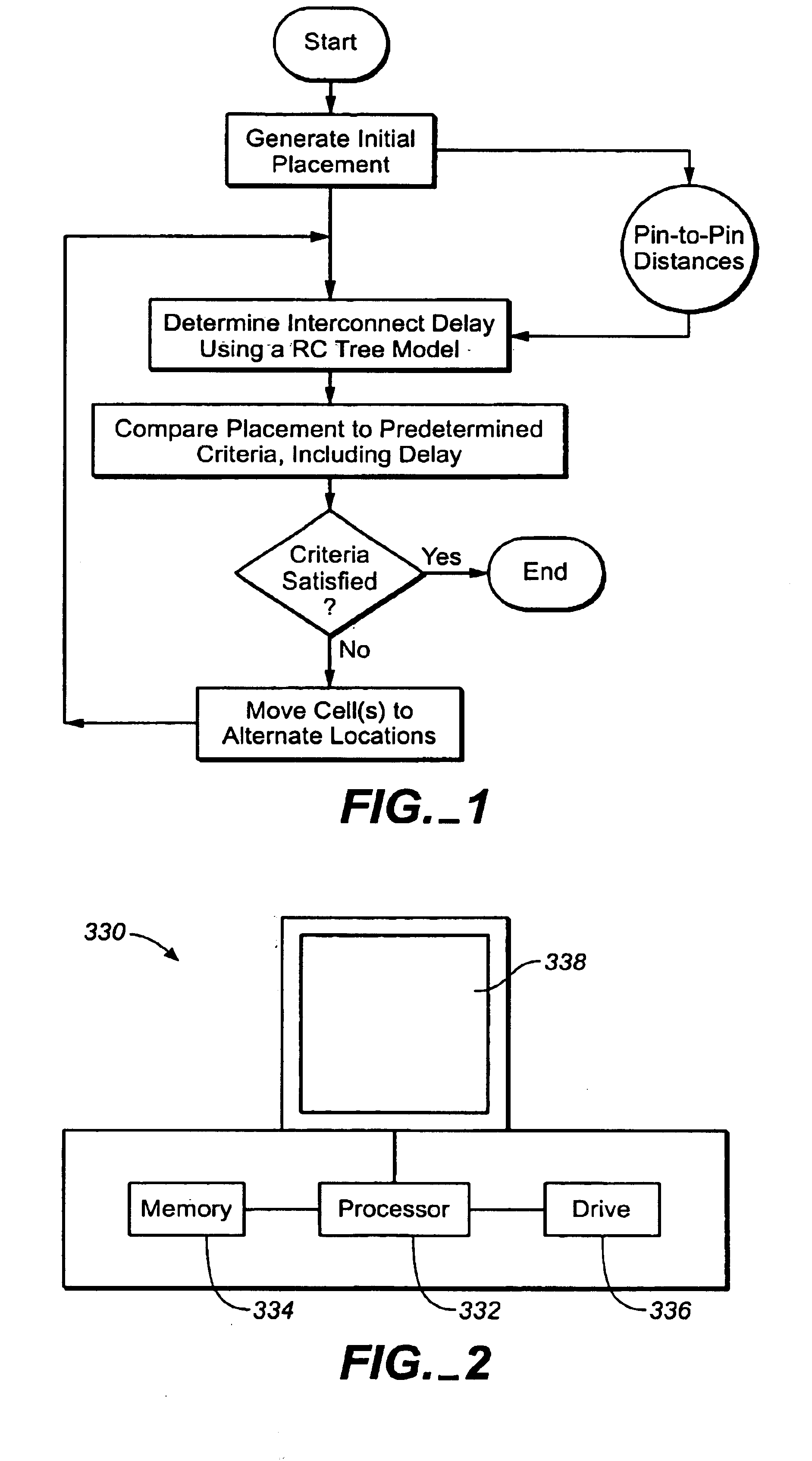
[0023]As is shown by FIG. 1, a flowchart of a preferred version of the present invention, the method of the present invention generally comprises the steps of comparing a placement of cells to predetermined cost criteria and moving cells to alternate locations on the surface if necessary to satisfy the cost criteria. The cost criteria include a timing criterion based upon cell and interconnect delay, where interconnect delay is modeled as a RC tree. Preferred versions of the present invention utilize RC tree interconnect delay models that are consistent with timing models used at design levels above placement, such as synthesis, and below placement, such as routing. The interconnect delay models of the present invention are now described in greater detail.
[0024]Given a routing tree with a driver and a set of sinks, a grid is superimposed at the routing plane to segment the wire and the delay from the input of the driver to the input of any sink is computed as
Δ=ΔC+ΔINT (1)
where ΔC ...
PUM
 Abstract
Description
Claims
Application Information