

COG-assembly and connecting material to be used therein
a technology of chiponglass and connecting materials, which is applied in the direction of identification means, semiconductor/solid-state device details, instruments, etc., can solve the problems of deformation of the substrate glass board, local stress concentration at the interface between the acm and the acm, and the hardening contraction and local stress at the interface are greater than the local stress, so as to reduce the local stress concentration at the interface, and reduce the occurrence of deformation
Inactive Publication Date: 2005-06-07
DEXERIALS CORP
View PDF9 Cites 19 Cited by
- Summary
- Abstract
- Description
- Claims
- Application Information
AI Technical Summary
Benefits of technology
The present invention provides a COG assembly and a connecting material for bonding and connecting semiconductor chips with substrate glass boards in a COG assembly. The connecting material comprises an adhesive component and electroconductive particles, which can reduce stress concentration at the interfaces and prevent deformation of the assembly. The adhesive component can be a thermosetting resin or a microparticulate elastomer with an average particle size of 30-300 nm. The resulting COG assembly has superior bonding strength and maintains good electroconductive connection. The invention also provides a liquid crystal display with the COG assembly.
Problems solved by technology
The adhesive strength of the ACM onto the substrate glass board or onto the chip is supported by the hardening contraction of the thermosetting resin, which may, however, cause the occurrence of local stress concentration at the interface between the ACM and the substrate glass board or the IC chip.
For attaining a high adhesive strength for the ACM, a thermosetting resin capable of building up a cured mass having a high elastic modulus may be chosen, which may bring about, however, greater hardening contraction and higher local stresses at the interfaces.
While these local stresses remain as residual stress within the resin layer when the thickness of the substrate glass board is large, they may cause a deformation of the substrate glass board, such as warping or the like, when the glass board is thin.
Use of a thin glass board may favor the occurrence of deformation of the bonded assembly, resulting in deterioration of the display performance in the case of an LCD.
Method used
View moreImage
Smart ImageViewing Examples

Examples
examples
[0049]Below, the present invention will further be described by way of embodiments with reference to the drawings appended.
Login to View More PUM
| Property | Measurement | Unit |
|---|---|---|
| tensile elongation percentage | aaaaa | aaaaa |
| particle size | aaaaa | aaaaa |
| particle size | aaaaa | aaaaa |
Abstract
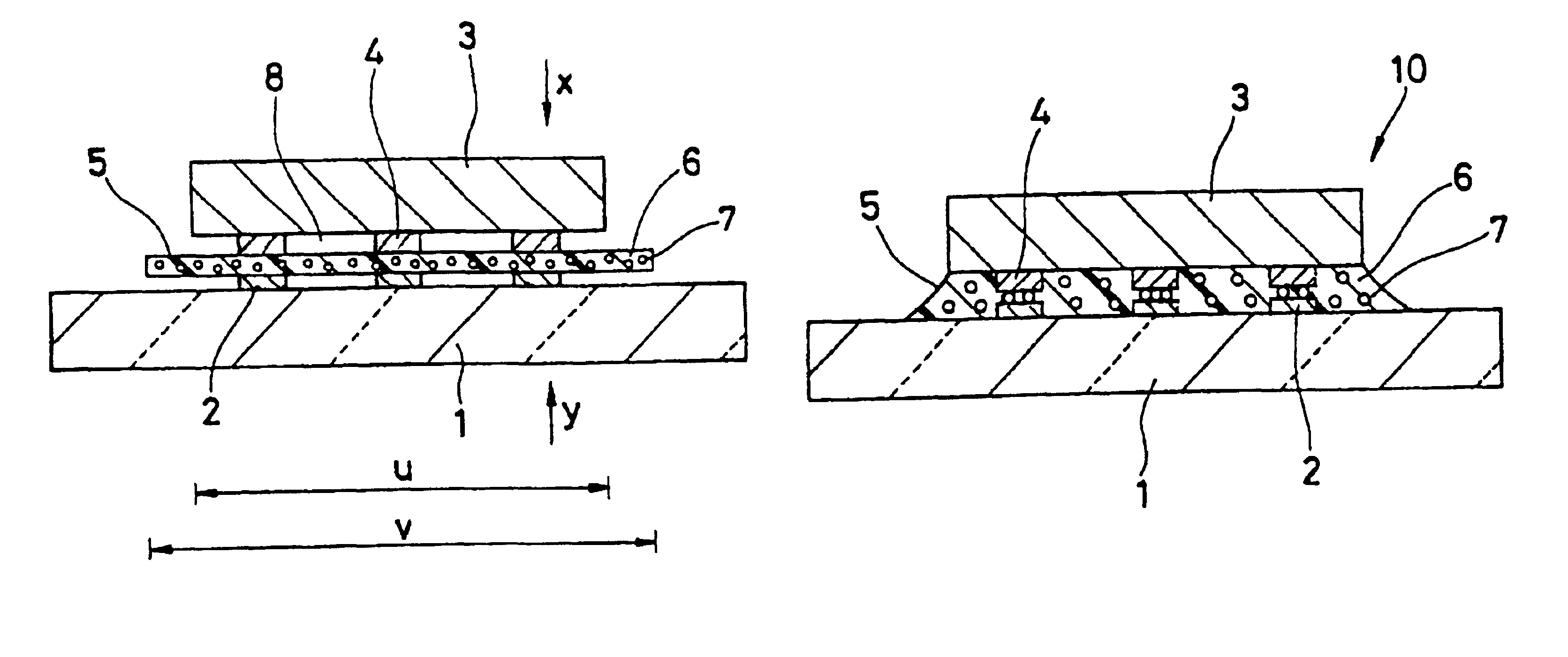
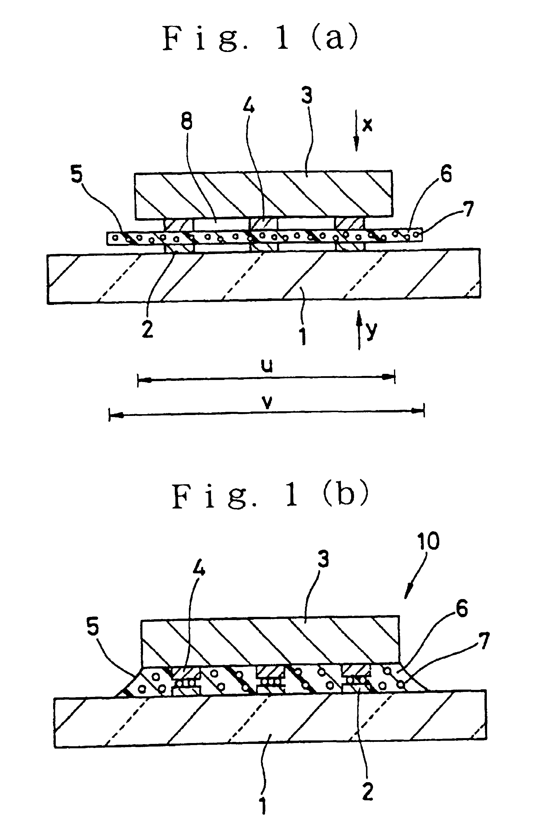
A chip-on-glass (COG) assembly, in which the electrodes of the semiconductor chips (3) are held in direct connection with the corresponding electrodes on the substrate glass circuit board (1), utilizes a layer (5) of a connecting material for bonding and connecting the semiconductor chip (3) with the substrate board (1). The connecting material can provide a reduced stress concentration at the boundaries between the binder layer (5) and the chip (3) and between the binder layer (5) and the glass board (1), even at higher adhesive strengths, bringing about less deformation, such as warping, of the resulting bonded assembly, even when using a thinner substrate glass board, and provides a superior bonding strength and excellent electroconductive performance. The connecting material is made up of, on the one hand, an adhesive component (6) containing a thermosetting resin and, on the other hand, electroconductive particles (7) and has a characteristic feature that a tensile elongation percentage at 25° C., after having been cured, is at least 5%.
Description
FIELD OF THE INVENTION[0001]The present invention relates to a chip-on-glass (COG) assembly in which semiconductor chip(s) are bonded and connected to a substrate glass circuit board directly, especially that to be used, for example, for liquid crystal displays, and to a connecting material to be used therein.DESCRIPTION OF THE RELATED TECHNIQUES[0002]In the past, liquid crystal displays (in the following referred to sometimes as LCD) are constituted by installing a semiconductor package, such as driver IC etc., on a substrate glass circuit board. However, from the recent general trend of fondness for light, thin, short and small articles, it has become a practice of producing liquid crystal displays by using a COG assembly made by assembling the semiconductor chip on a glass substrate board with direct connection thereto. In such a COG assembly, the correspondingly confronting electrodes on the substrate glass circuit board and on the chip are connected together using an anisotropi...
Claims
Login to View More Application Information
Patent Timeline
 Patent Type & AuthorityPatents(United States)
IPC IPC(8): H01L21/56H01L21/02H01L21/60H05K3/32H01R11/01C09J9/02C09J201/00G09F9/00H01R4/04H01R4/58
CPCC09J11/00H01L21/563H01L24/83C09J9/02H01L24/29C08K9/02Y10T428/254C09J2433/00C09J2461/00G02F1/13452H01L2224/16225H01L2224/73203H01L2224/73204H01L2224/83101H01L2224/8319H01L2224/838H01L2924/01004H01L2924/01005H01L2924/01027H01L2924/01033H01L2924/01039H01L2924/01049H01L2924/0105H01L2924/01077H01L2924/01078H01L2924/01079H01L2924/04953H01L2924/0781H01L2924/14H05K3/323H01L2924/01006H01L2924/01019H01L2924/01023H01L2924/01024H01L2924/01045H01L2924/014H01L2924/0665H01L2224/83851H01L2224/2929H01L2924/00013Y10S428/901H01L2224/32225H01L2924/00H01L2924/00014H01L2224/29299H01L2224/29099H01L2224/29199H01R4/58
InventorTAKEICHI, MOTOHIDEFUJIHIRA, HIROYUKI
OwnerDEXERIALS CORP