Deterministic testing of edge-triggered logic

Inactive Publication Date: 2005-06-07
SAMSUNG ELECTRONICS CO LTD
View PDF14 Cites 42 Cited by
  • Summary
  • Abstract
  • Description
  • Claims
  • Application Information

AI Technical Summary

Benefits of technology

[0017]The present invention provides a technique of testing logic incorporating edge-triggered devices incorporated in at least two clock domains that resolves timing and skew pro

Problems solved by technology

At times, a pseudo-random test will not adequately test some portion of the circuit under test.
These operating conditions include the manufacturing process variations of the circuit, the test voltage, and the test temperature, all of which influence the logic delay of the circuit under test.
Without this feature of determinism, scan testing cannot be relied upon.
This problem is exacerbated when multiple clock inputs, such as CLK1, .
Test coverage is likely to be poor because of low controllability and observability, unless a major investment is made in functional test vector development.
The interfaces between the clock domains, which were formerly asynchronous, may now have short-path problems which will cause unreliable/unrepeatable scan test results.
This problem arises because, as is conventional, edge-triggered devices will accept and latch data applied to the input on one edge of the applied clock.
However, a latch-based design is not the technology of choice for some integrated circu

Method used


Image

  • Deterministic testing of edge-triggered logic
  • Deterministic testing of edge-triggered logic
  • Deterministic testing of edge-triggered logic

Examples


Embodiment Construction

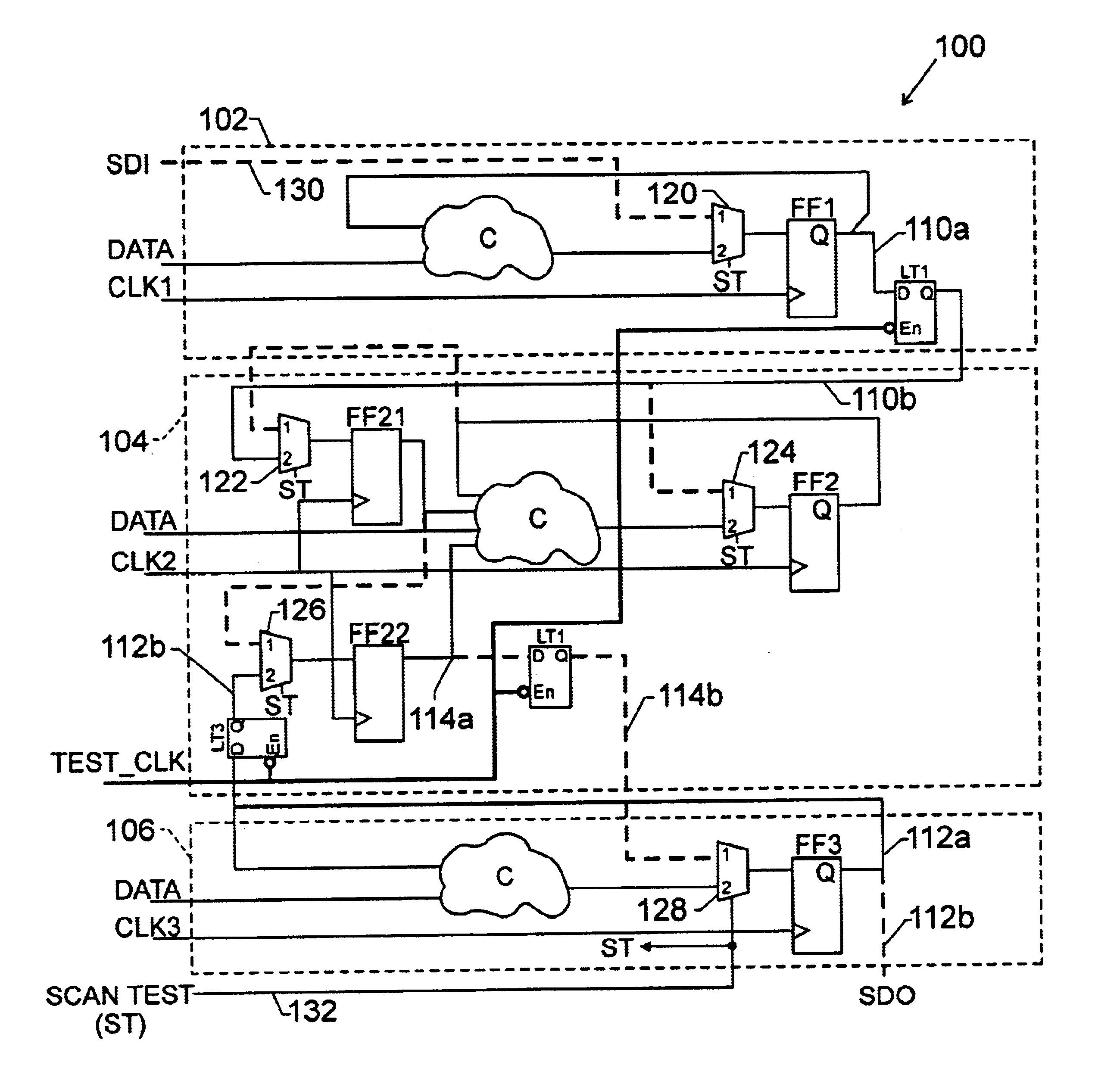
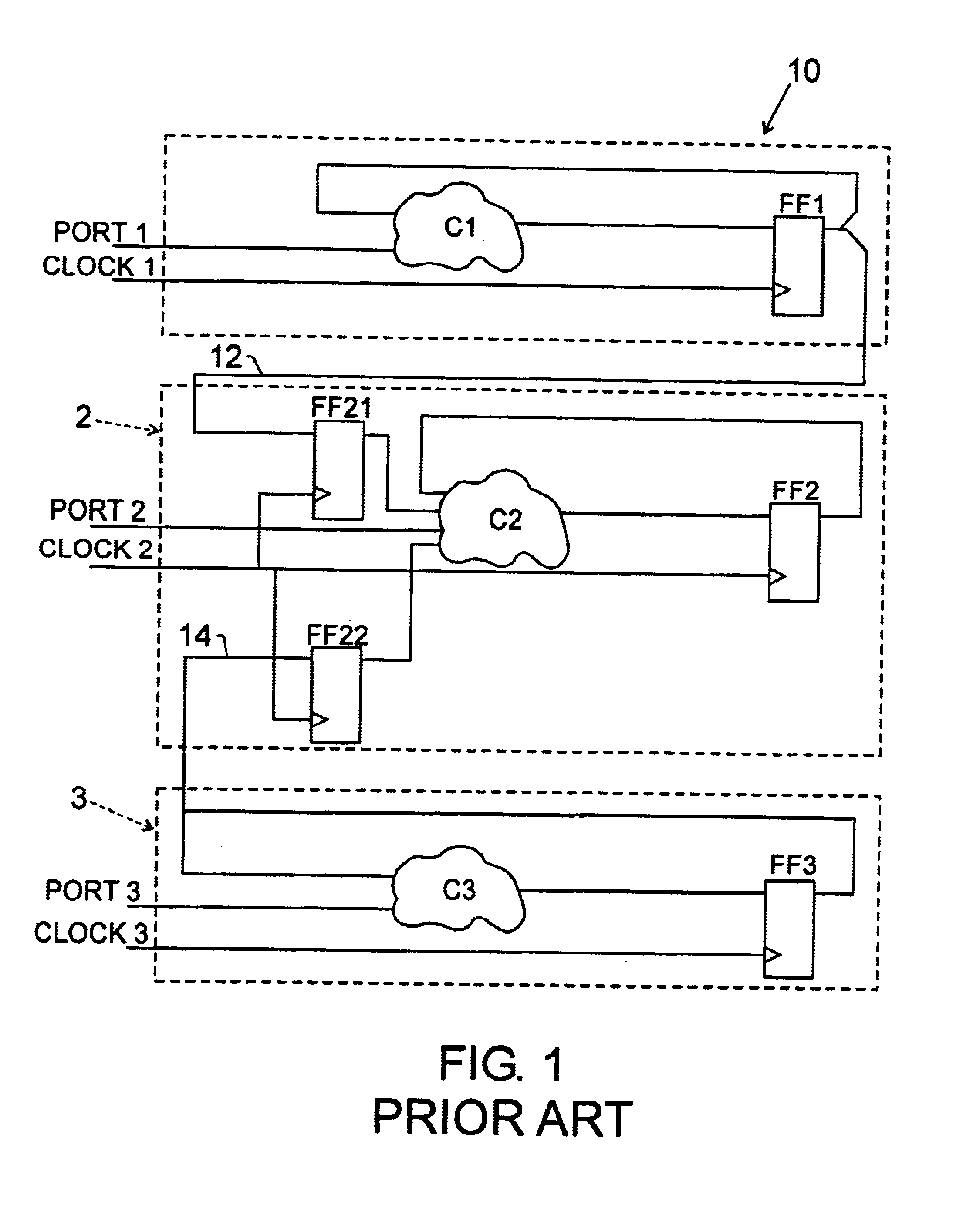
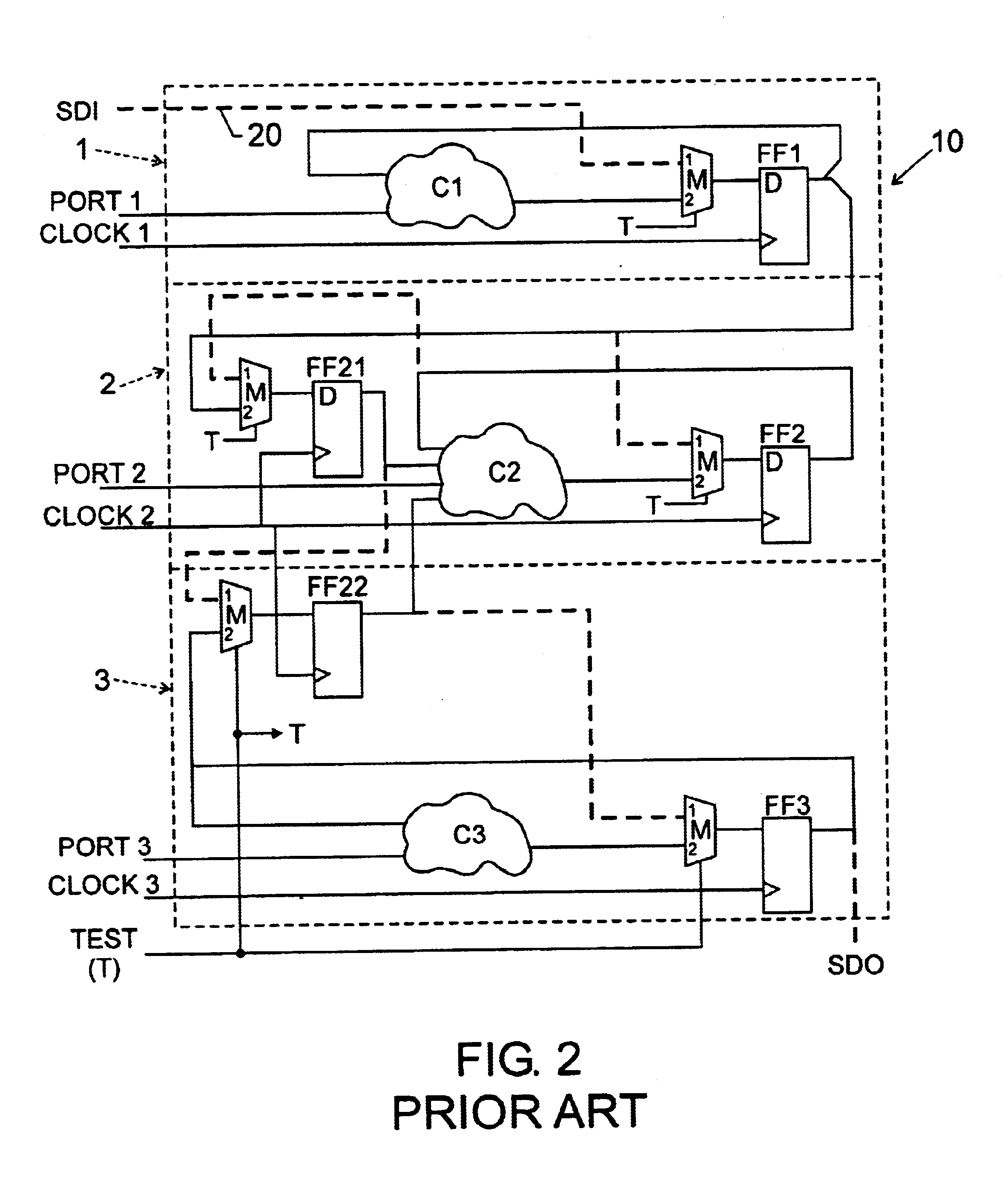
[0034]Turning now to FIG. 3, there is illustrated the circuit 100, which is, in effect, a modified version of the circuit 10′ of FIG. 2, incorporating an embodiment of the present invention. As FIG. 3 shows, the circuit 100 includes, as did circuit 100, three clock domains 102, 104, and 106. Each clock domain includes data (DATA) and clock (CLK) inputs, combinatoral logic C, and representative clocked, edge-triggered devices such as the flops FF1 (clock domain 102), F2, FF21, and FF22 (clock domain 104), and FF3 (clock domain 106). Multiplexers 120, 122, . . . , 128 are provided in the circuit 100 to allow formation of a selectable scan path between an SDI input on signal line 130 to a SDO output line 112b in response to assertion of a test signal (SCAN TEST (ST) on signal line 132.

[0035]When operating normally (i.e., in its functional state), data produced by the flop FF1 of clock domain 102 is communicated from its Q output to the clock domain 104 (as well as back to the combinato...


PUM


Abstract

A digital system having multiple clock domain, each including at least one edge-triggered device, such as a flip-flop, is structured to be submitted to scan testing. Each data path from one clock domain to another includes a latch that is operated by a test clock. During scan testing, when the digital system is logically reconfigured to form one or more scan chains for receiving a test vector, the latches are operated to ensure that the test vector is passed from one domain to another.

Description

BACKGROUND OF THE INVENTION[0001]The present invention relates generally to testing digital logic, and more particularly to a logical and consistent method and mechanism for using scan test techniques to test edge-triggered logic in a manner that resolves timing problems.[0002]Recent advances in integrated circuit fabrication for digital systems has resulted in significant increases in the circuit density. Techniques for testing such high-density integrated circuitry have also advanced in order to be able to provide a credible assessment of the operability of an integrated circuit and systems incorporating integrated circuits. These techniques strive to produce a test methodology that can produce a reliable assessment in a minimum amount of time.[0003]One such test technique enjoying relatively popular use today, sometimes termed “scan testing,” involves implanting a digital test state in the circuit under test and allowing it to operate normally before extracting and examining the ...

Claims


Application Information

Patent Timeline
IPC IPC(8): G01R31/28G01R31/3185
CPCG01R31/318594
Inventor BROWN, JOHN MICHAEL
Owner SAMSUNG ELECTRONICS CO LTD
Why Eureka
Try Eureka