Method of manufacturing semiconductor device

a manufacturing method and semiconductor technology, applied in the direction of manufacturing tools, soldering devices, printed circuit boards, etc., can solve the problems of voids, voids, and gasses generated by flux vaporization, and achieve the effect of removing warping and increasing creep

Inactive Publication Date: 2005-06-14
FUJI ELECTRIC CO LTD
View PDF12 Cites 7 Cited by
  • Summary
  • Abstract
  • Description
  • Claims
  • Application Information

AI Technical Summary

Benefits of technology

[0018]The furnace can be evacuated and then positively pressurized with the hydrogen gas to reduce at least the surfaces of the laminate to be bonded before heating the laminate to the bonding temperature. The laminate can be heated to the bonding temperature to melt the solder sheet while maintaining the atmosphere of hydrogen gas under the positive pressure. The hydrogen gas fills the voids produced in the liquefied solder when the solder sheet is melting to activate the voids.
[0019]The furnace can be evacuated while maintaining the bonding temperature to remove the voids in the liquefied solder. Thereafter, the furnace can be pressurized again with hydrogen gas to a positive pressure, while maintaining the bonding temperature to prevent holes produced by the voids traveling in the liquefied solder, and to uniformly shape a solder fillet thereof. Thereafter, the laminate can be rapidly cooled in the furnace while maintaining the atmosphere of hydrogen gas under the positive pressure. During the cooling step, the solder can be formed with a finer grain by increasing a rate of creep to remove warping of the laminate due to differences in the coefficient of thermal expansion among different components of the laminate. In this respect, the rate of cooling can be maintained at 250° C. or higher per minute. More specifically, the rate of cooling can be maintained at 300° C. or higher per minute. Moreover, the hydrogen gas can be evacuated from the furnace and an atmosphere of nitrogen gas can be pressurized to a positive pressure before opening the furnace. More specifically, the atmosphere of hydrogen gas in the furnace can be replaced with the atmosphere of nitrogen gas when the laminate reaches a temperature of 60° C. or below.

Problems solved by technology

Presence of voids in a solder between the silicon chip and the insulator substrate or between the insulator substrate and the metal base prevents heat dissipation, which can damage the semiconductor device.
One of the causes of formation of voids in the solder bonded layer is that gas, such as carbon dioxide gas, dissolved in the solder material remains in the voids formed in the solder when the solder melts.
Another cause is that gasses generated by the flux vaporization also can form voids.
Moreover, the flux itself remaining in the solder bonded layer can form voids.
Here, however, no reduction gas, such as hydrogen gas, is used.
In the above-described first to third methods of manufacturing power semiconductor devices, however, following problems exist.
Because the silicon chips are handled many times, probability of damaging silicon chips is increased, which can degrade electric characteristics.
The produced warping creates nonuniform stress in the silicon chip at wire bonding, which can degrade electric characteristics.
Contaminants, such as residues left after cleaning, adhered on the surface of the silicon chip can degrade electric characteristics, such breakdown voltage.
Thus, it can degrade reliability.
Moreover, differences in heat capacity among different materials fed into the furnace necessitate control of temperature in the furnace whenever a material is fed.
Moreover, in the methods of manufacturing power semiconductor device by the above-explained first to third methods, the following heat dissipation problem exists.
Therefore, the voids are liable to be left in solder bonded layers.
This, however, raises the cost of the materials.
Moreover, precise control is required for an oxygen concentration, a dew point, and a temperature profile in the soldering furnace, which all significantly increase the operation cost of the soldering furnace.
Furthermore, in the third method, insufficient depressurization leaves traces of removed fluxes, i.e., traces of traveled fluxes, and voids in the solder bonded layer.
In addition, removal of all the fluxes by depressurization is very time consuming, thus decreasing productivity in the case of a batch furnace.
This necessitates frequent cleaning of the inside of the apparatus, again raising the cost of maintaining and controlling the apparatus.
Further, soldering carried out at 300° C. or higher causes sticking of scorched flux.
Thus, soldering is limited to below 300° C.

Method used


Image

  • Method of manufacturing semiconductor device
  • Method of manufacturing semiconductor device
  • Method of manufacturing semiconductor device

Examples


Embodiment Construction

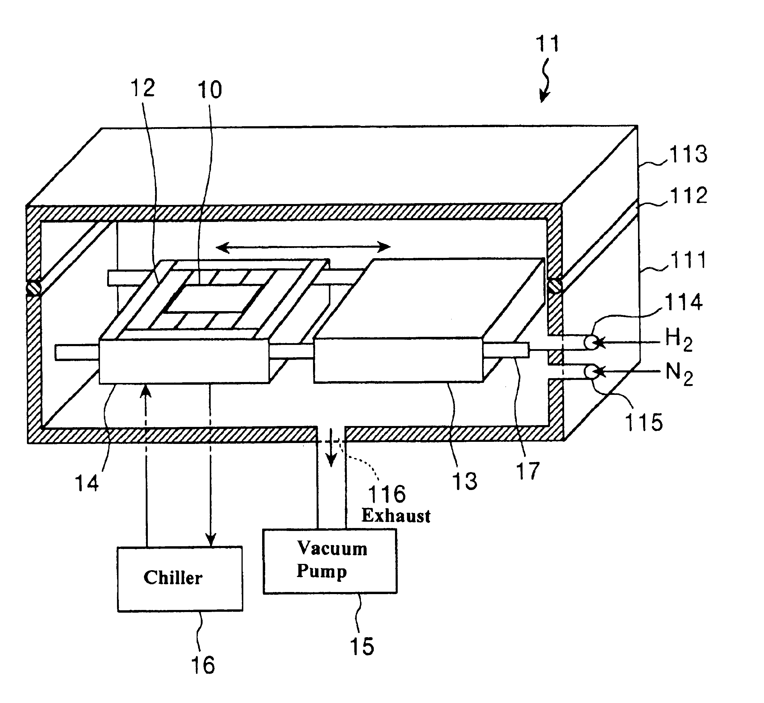
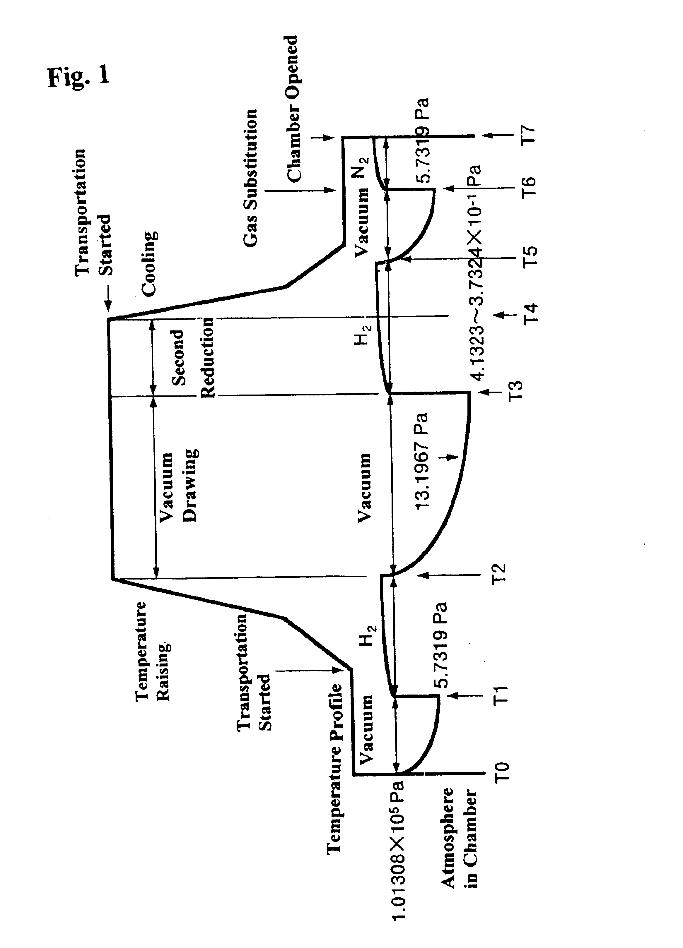
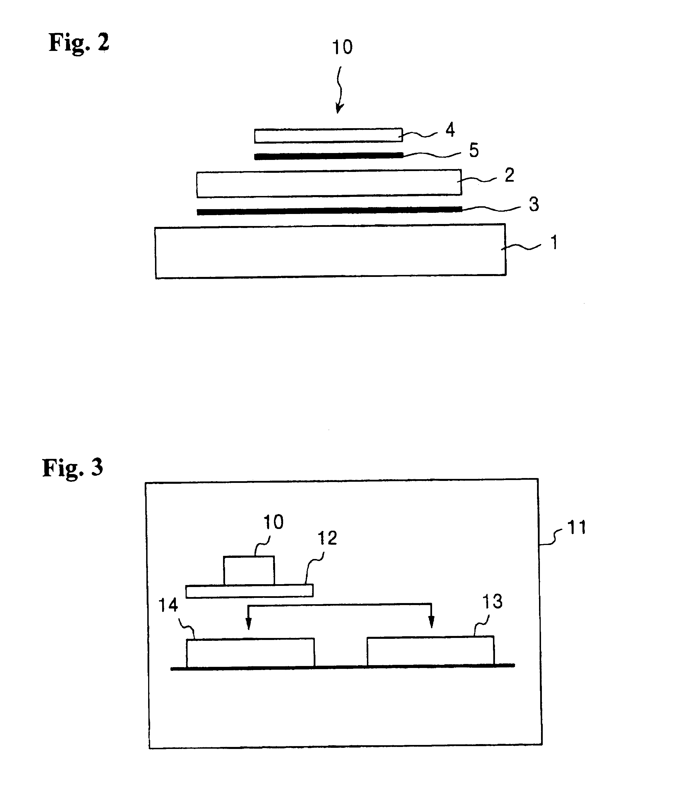
[0043]The present invention is explained in detail with reference to the drawings. FIG. 1 is a chart showing an example of a temperature profile, atmospheres, and pressures in a chamber and a processing operation in the method of manufacturing a semiconductor device according to the present invention. First, as shown in FIG. 2, the components to be soldered and bonded are prepared by stacking an insulator substrate 2 on a metal base 1 with a bonding solder sheet 3 sandwiched therebetween. On the insulator substrate 2, a silicon chip 4 is further stacked with another bonding solder sheet 5 sandwiched therebetween. Such a laminate or stack 10, as shown in FIG. 3, is positioned on a transport stage 12 of a reduced pressure furnace 11. The transport stage 12 is a configured to move back and forth between a hot plate 13 for heating the laminate 10 and a water cooling plate 14 for cooling the laminate 10.

[0044]When soldering is started according to the chart shown in FIG. 1, with the lami...


PUM

PropertyMeasurementUnit
temperatureaaaaaaaaaa
total lengthaaaaaaaaaa
flow rateaaaaaaaaaa

Abstract

A semiconductor device can be formed with fewer voids in the solder bonding a laminate of a silicon chip, an insulator substrate, and a metal base, with a solder layer positioned between the layers. After placing the laminate in a furnace, it is evacuated and then pressurized with hydrogen gas, and then heated to melt the solder. While maintaining the heat, the furnace is again evacuated to remove voids in the solder, and then the furnace is positively pressurized again with hydrogen gas to prevent holes produced by the voids traveling in the solder, and to obtain a uniform solder fillet shape. Thereafter the laminate is rapidly cooled to obtain a finer grain solder to increase the rate of creep to quickly remove the warping of the laminate to the original state.

Description

BACKGROUND[0001]In a power semiconductor device, soldering is achieved by one of the following three ways. In the first method, preliminary soldering is formed in a continuous furnace (a tunnel furnace) in a reducing atmosphere to provide solder on electrodes on a bottom face of a silicon chip. Subsequently, the silicon chip is soldered on an insulator substrate with the solder placed between them. Afterward, wire bonding is done. Then, an element with the silicon chip soldered on the insulator substrate is soldered in the atmosphere onto a metal base made of copper using a flux. In the second method, a silicon chip and an insulator substrate are soldered using the continuous furnace in a reducing atmosphere. Afterward, wire bonding is carried out. Then, an element with the silicon chip soldered on the insulator substrate is soldered onto a metal base using the continuous furnace in the reducing atmosphere. In the third method, by using a reduced pressure furnace in an inert atmosph...

Claims


Application Information

Patent Timeline
Patent Type & Authority Patents(United States)
IPC IPC(8): B23K1/00B23K1/20B23K1/008H01L21/02H01L21/58H05K3/00H05K3/34H05K1/03B23K31/02B23K101/40H01L21/52
CPCB23K1/0016B23K1/008H01L24/75H01L24/32B23K1/206H01L24/83H01L2924/10253H01L2224/29111H01L2924/1579H01L2924/15787H01L2924/0132H01L2924/014H01L2924/01006H05K3/341H05K3/0058H05K1/0306H01L2924/3025H01L2924/07802H01L2924/01082H01L2224/32145H01L2224/83101H01L2224/8319H01L2224/8385H01L2924/01004H01L2924/01029H01L2924/01033H01L2924/01047H01L2924/0105H01L2924/01074H01L2924/01075H01L2924/01078H01L2924/3512H01L2924/00H01L2924/00014H01L2224/83815
Inventor MOROZUMI, AKIRAMIYASAKA, TADASHIYAMADA, KATSUMIMOCHIZUKI, EIJI
Owner FUJI ELECTRIC CO LTD
Why Eureka
Try Eureka