Versatile method and system for single mode VCSELs

a single-mode vcsel and output mode technology, applied in the field of semiconductor lasers, can solve the problems of multiple-mode source inefficiency or unusability, difficult to manufacture vcsels that efficiently operate in the lower range, and negative effects on the output mode of a semiconductor laser, so as to maximize the loss, commercially viable vcsel power output and performance, and cost-effective and efficient

Inactive Publication Date: 2005-06-14
II VI DELAWARE INC
View PDF179 Cites 12 Cited by
  • Summary
  • Abstract
  • Description
  • Claims
  • Application Information

AI Technical Summary

Benefits of technology

[0009]In the present invention, electrical thermal and geometric optical properties of VCSEL components are designed and selected to provide current peaking in the center of a VCSEL device, coincident with the peak of the lowest order mode and to maximize loss in, or eliminate completely, higher order modes. Optionally, other mode control techniques can be used in conjunction with the teachings of the present invention to optically tailor the loss profile to prefer the fundamental mode.

Problems solved by technology

Depending upon the application, the output mode of a VCSEL can either positively or negatively affect its use in signal transmission and other applications.
This can present problems in signal communications applications where transmission depends on a consistent and reliable signal.
Other applications (e.g., printing devices, analytical equipment) may require a consistent and focused light source or spectral purity characteristics that render multiple mode sources inefficient or unusable.
Manufacturing a VCSEL with mode control and high performance characteristics poses a number of challenges.
It is difficult to manufacture VCSELs that efficiently operate in the lower order mode (single mode).
Conventional attempts to produce a single mode VCSEL have generally resulted in structures having output power insufficient for practical use in most applications, as they remain single mode only over small current ranges.
A problem with a large current aperture is that higher order lasing modes are introduced so that single mode lasing only occurs just above threshold, if at all.
Manufacturing a VCSEL with a smaller current aperture to obtain single mode behavior causes multiple problems: the series resistance becomes large, the beam divergence angle becomes large, and the attainable power becomes small.
Some conventional anti-guide structures may achieve this but suffer from manufacturing difficulties, particularly in requiring an interruption in epitaxial growth, a patterning step, and subsequent additional epitaxy.
Other large single mode VCSELs require multi-step MBE or MBE / MOCVD combinations to manufacture, creating alignment and yield problems; increasing production costs and reducing commercial viability.

Method used


Image

  • Versatile method and system for single mode VCSELs
  • Versatile method and system for single mode VCSELs
  • Versatile method and system for single mode VCSELs

Examples


Embodiment Construction

[0021]While the making and using of various embodiments of the present invention are discussed in detail below, it should be appreciated that the present invention provides many applicable inventive concepts which can be embodied in a wide variety of specific contexts. The specific embodiments discussed herein are merely illustrative of specific ways to make and use the invention and do not delimit the scope of the invention.

[0022]It should be understood that the principles and applications disclosed herein can be applied in a wide range of optoelectronic applications. For purposes of explanation and illustration, the present invention is hereafter described in reference to VCSEL laser sources. However, the same system might be applied in other applications where a single mode source is utilized.

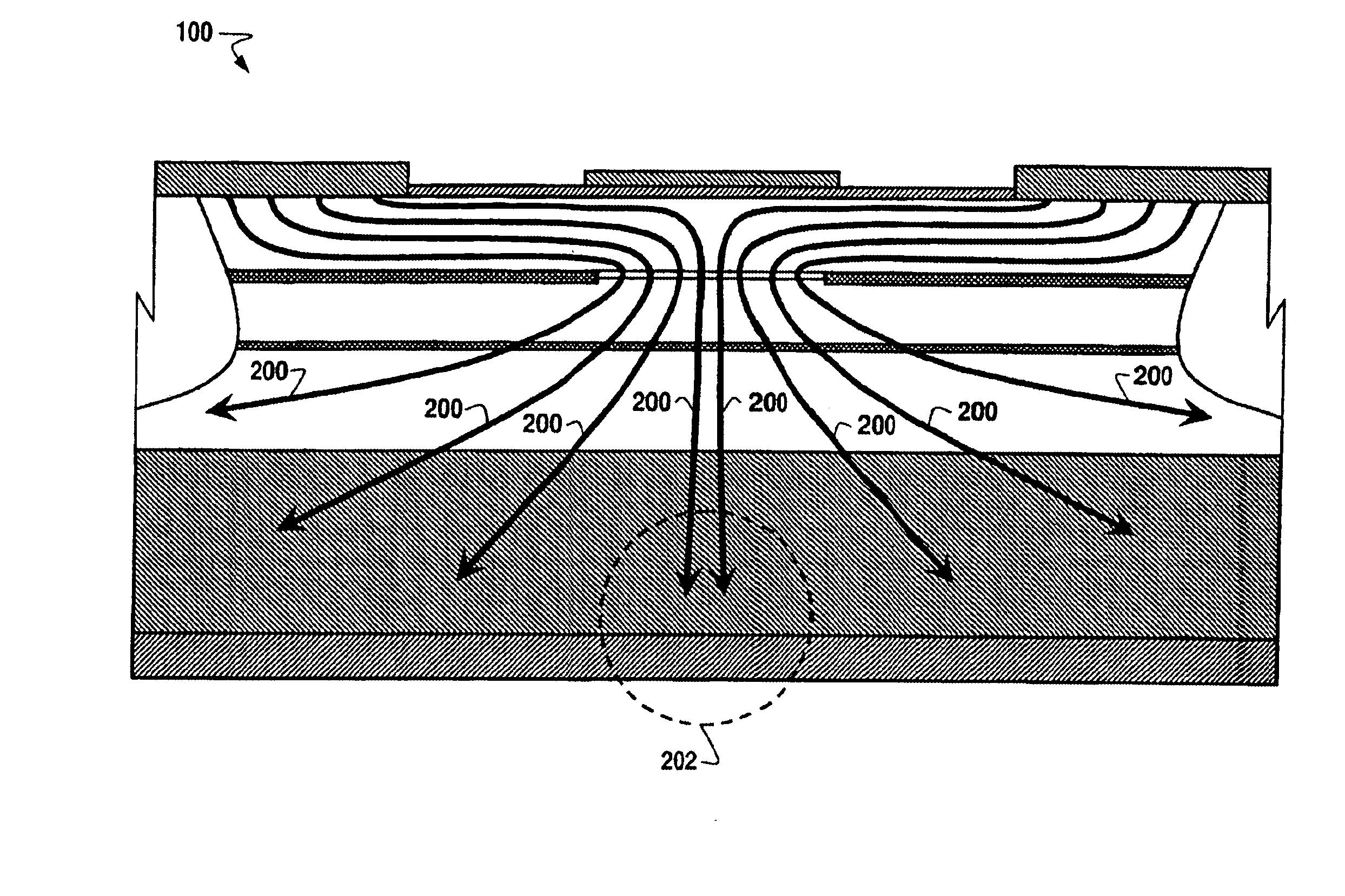
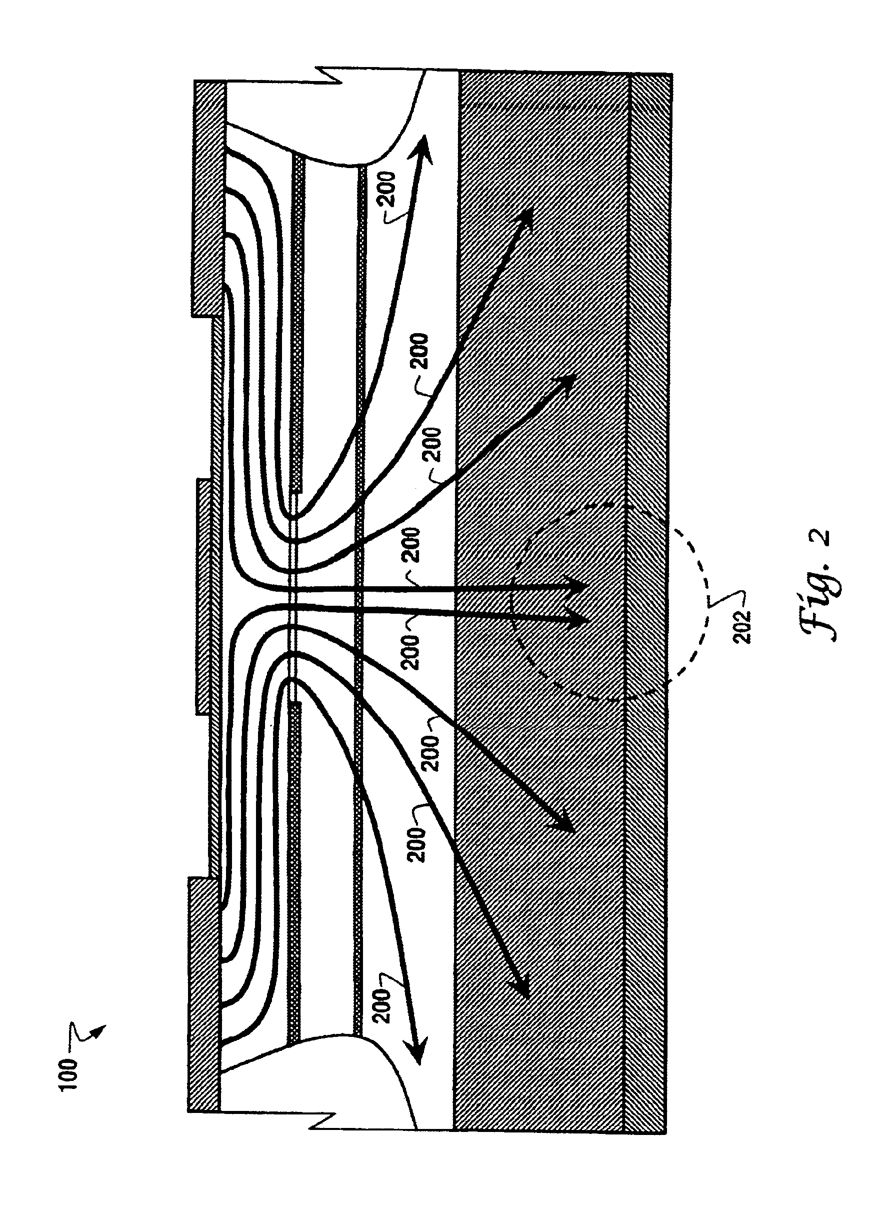
[0023]As previously discussed, one of the limitations of conventional single mode VCSEL approaches is their tendency to become multi-moded as current is increased, resulting in a very small ...


PUM


Abstract

A system and method for providing a single mode VCSEL (vertical cavity surface emitting laser) component (100) is disclosed, comprising a semiconductor substrate (102) having a lower surface and an upper surface, a bottom electrical contact (104) disposed along the lower surface of the substrate, a lower mirror (106) formed of n-type material and disposed upon the upper surface of the substrate, an active region (108) having a plurality of quantum wells disposed upon the lower mirror portion, an upper mirror (110) formed from isotropic material and disposed upon the active region, an equipotential layer (112) disposed upon the upper mirror portion, a first upper electrical contact (120) disposed upon the equipotential layer, a second upper electrical contact (122) disposed upon the equipotential layer at a particular distance (124) from the first upper electrical contact, a first isolation region (126) disposed beneath the first upper contact and traversing the equipotential layer, the upper mirror, the active region, and the lower mirror, a second isolation region (128) disposed beneath the second upper contact and traversing the equipotential layer, the upper mirror, the active region, and the lower mirror, and an insulating layer (114, 116) interposed between the upper mirror and the equipotential layer and adapted to form therebetween an aperture (118) of smaller dimension than the particular distance between the first and second upper contacts.

Description

TECHNICAL FIELD OF THE INVENTION[0001]The present invention relates, in general, to semiconductor lasers and, in particular to a versatile system for producing single transverse mode Vertical-Cavity Surface-Emitting Lasers (VCSELs).BACKGROUND OF THE INVENTION[0002]The Vertical Cavity Surface Emitting Laser (VCSEL) is rapidly becoming a workhorse technology for semiconductor optoelectronics. VCSELs can typically be used as light emission sources anywhere other laser sources (e.g. edge emitting lasers) are used, and provide a number of advantages to system designers. Hence, VCSELs are emerging as the light source of choice for modern high-speed, short-wavelength communication systems and other high-volume applications such as optical encoders, reflective / transmissive sensors and optical read / write applications.[0003]Surface-emitting lasers emit radiation perpendicular to the semiconductor substrate plane, from the top or bottom of the die. A VCSEL is a surface-emitting laser having mi...

Claims


Application Information

Patent Timeline
Patent Type & Authority Patents(United States)
IPC IPC(8): H01S5/00H01S5/183H01S5/20H01S5/042H01S5/028
CPCH01S5/18391H01S5/18308H01S5/18311H01S5/18316H01S2301/166H01S5/18377H01S5/2063H01S5/18369H01S5/183
Inventor JOHNSON, RALPH H.MORALES, GILBERTO
Owner II VI DELAWARE INC
Why Eureka
Try Eureka