FET amplifier with temperature-compensating circuit

a technology of temperature compensation and amplifier, applied in the direction of amplifier, amplifier with semiconductor devices only, amplifier with discharge tubes, etc., can solve the problems of wide difference, large variation in operating current (drain current), and large variation in susceptibility to distortion, so as to minimize the worsening of distortion susceptibility

Inactive Publication Date: 2005-06-14
NEC CORP
View PDF4 Cites 51 Cited by
  • Summary
  • Abstract
  • Description
  • Claims
  • Application Information

AI Technical Summary

Benefits of technology

[0021]The FET amplifier with temperature-compensating circuit according to the invention has the advantage of being capable of keeping the drain current amperage of the LDMOS FET amplifier constant and thereby minimizing the worsening of the dist

Problems solved by technology

At the same time, this device has a disadvantage that its operating current (drain current) greatly varies with the ambient temperature of operation and its susceptibility to distortion also greatly varies with the fluctuations of this drain current.
As a result, a wide difference may arise between the consumed amperage at the normal temperature an

Method used


Image

  • FET amplifier with temperature-compensating circuit
  • FET amplifier with temperature-compensating circuit
  • FET amplifier with temperature-compensating circuit

Examples


Embodiment Construction

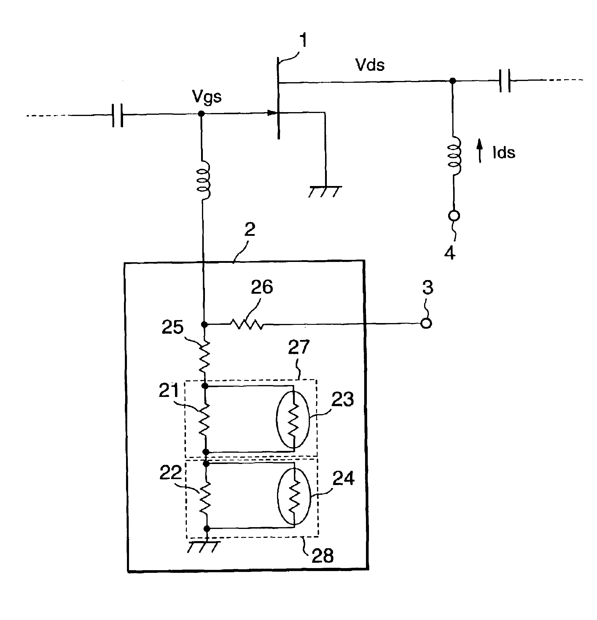
[0034]First will be explained variations in drain current dependent on the ambient temperature of operation of an LDMOS FET. FIG. 3 is a characteristic diagram showing variations in drain current relative to the gate voltage with the ambient temperature Ta of operation as the parameter. Vgs and Ids are normalized with their respective values at Ta=1+25° C. According to FIG. 4, if Vgs is fixed at abnormal value of 1, i.e. if no temperature compensation is applied, the drain current Ids will fluctuate as much as from −38% at Ta=−10° C. to +71% at Ta=+80° C.

[0035]Next will be explained the distortion-susceptibility of the LDMOS FET. FIG. 4 illustrates an example of the characteristic of third order cross modulation distortion (IM3) of the LDMOS FET. As FIG. 4 shows, there is a value of the drain current Ids at which IM3 is minimized (optimized), and IM3 steeply rises as this drain current Ids drops. Therefore, even if the distortion-susceptibility is set at the optimal point at the sta...


PUM


Abstract

A FET amplifier which minimizes the worsening of the distortion-susceptibility due to variations in the ambient temperature of operation is to be provided. An LDMOS FET 1, whose source terminal is grounded and to which are applied a gate voltage Vgs from a gate bias terminal 3 via a temperature-compensating circuit 2 and a choke coil and a drain voltage Vds from a drain bias terminal 4 via a choke coil operates as a source-grounded type amplifier. In the temperature compensating circuit 2, the resistances of fixed resistance elements 21 and 22 connected in parallel are set to be the same or have the same number of digits, and those of thermosensitive resistance elements (thermistors) 23 and 24 are set to be a combination of a value greater by one digit and a value smaller by one digit than that of the fixed resistance element 21 or the fixed resistance element 22 at the standard level (+25° C.) in the ambient temperature range of operation.

Description

BACKGROUND OF THE INVENTION[0001]1. Field of the Invention[0002]The present invention relates to a FET amplifier, and more particularly to a FET amplifier capable of minimizing the degradation of distortion in the output power due to temperature variations in the operating ambience.[0003]2. Description of the Related Prior Art[0004]As a device for use in a high-output amplifier in microwave band communication apparatuses, an LDMOS FET (lateral diffused MOS field effect transistor) is being increasingly adopted. This device has an advantage of having better output distortion characteristics than a GaAs FET (gallium arsenide field effect transistor) which can generally provide a high output more easily. For this reason, it is suitable for use in wireless base stations of the W-CDMA (Wideband Coded Division Multiple Access) type. At the same time, this device has a disadvantage that its operating current (drain current) greatly varies with the ambient temperature of operation and its s...

Claims


Application Information

Patent Timeline
IPC IPC(8): H03F3/189H03F1/30H03F3/193
CPCH03F3/193H03F1/301
Inventor AMANO, SHIGERU
Owner NEC CORP
Why Eureka
Try Eureka