Multi-chip package (MCP) with a conductive bar and method for manufacturing the same

a technology of conductive bars and multi-chip packages, which is applied in the direction of semiconductor devices, semiconductor/solid-state device details, electrical apparatus, etc., can solve the problems of increased packaging thickness, increased manufacturing cost, poor heat dissipation, etc., and achieves the effect of preventing adhesive strength failure, increasing chip thickness and warpage of semiconductor chips

Inactive Publication Date: 2005-06-21
SAMSUNG ELECTRONICS CO LTD
View PDF15 Cites 350 Cited by
  • Summary
  • Abstract
  • Description
  • Claims
  • Application Information

AI Technical Summary

Benefits of technology

[0012]Therefore, the present invention prevents the adhesive strength failure due to the increased chip thickness and warpage of the semiconductor chip while simultaneously stacks the plurality of chips without several solder reflow steps.

Problems solved by technology

However, the stack packaging described above also has several drawbacks such as increased package thickness due to the insertion of the substrate, an increased manufacturing cost and poor heat dissipation, thereby limiting the stackable number of semiconductor chips.
However, since the semiconductor chips are electrically interconnected using the solder bumps, adhesive strength changes due to warpage of the stacked chips and chip alignment failures may occur during the chip stacking process.

Method used


Image

  • Multi-chip package (MCP) with a conductive bar and method for manufacturing the same
  • Multi-chip package (MCP) with a conductive bar and method for manufacturing the same
  • Multi-chip package (MCP) with a conductive bar and method for manufacturing the same

Examples


Embodiment Construction

[0017]Preferred embodiments of the present invention will be described below with reference to the accompanying drawings.

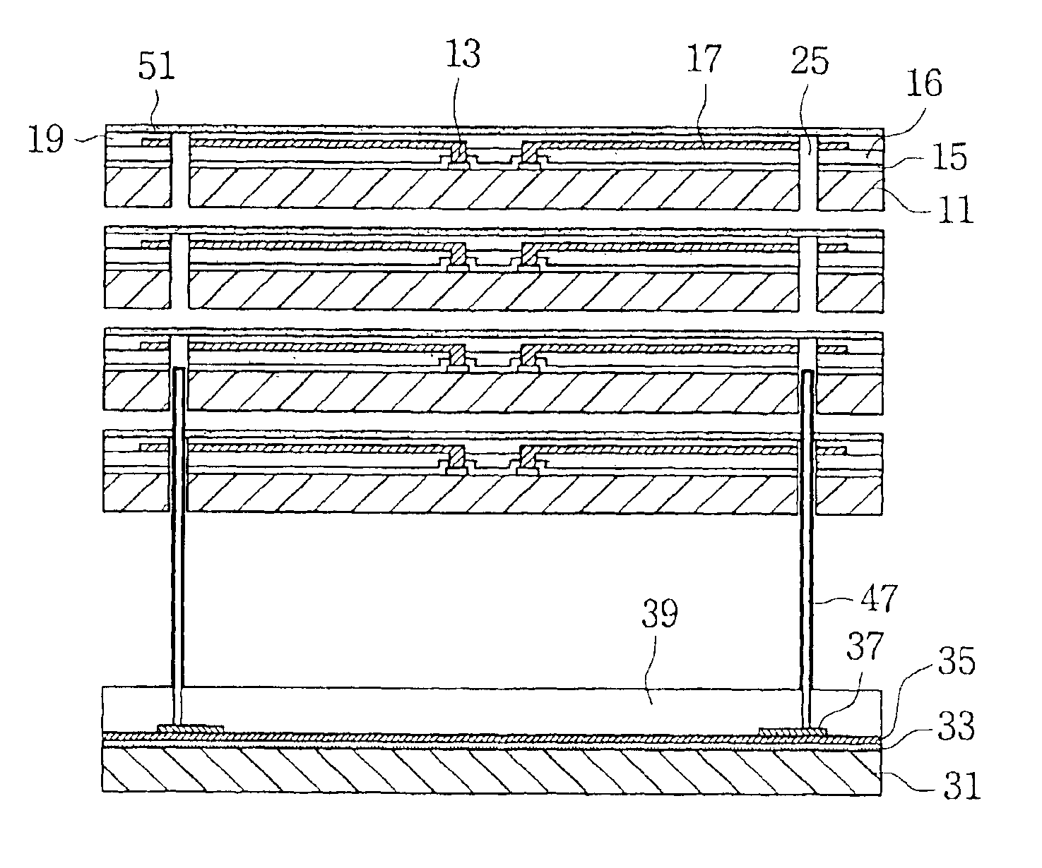
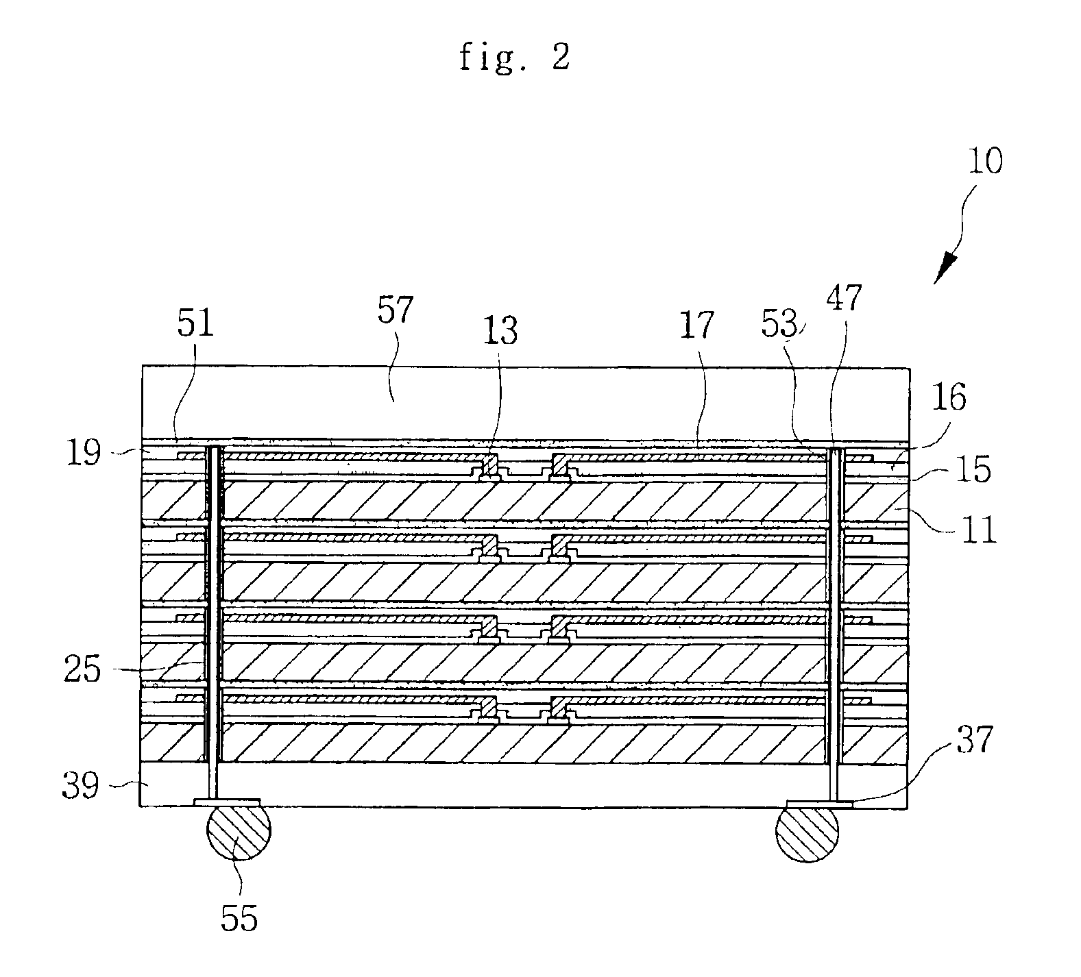
[0018]FIG. 2 is a cross-sectional view of a MCP in accordance with one embodiment of the present invention. Referring to FIG. 2, a MCP 10 has a plurality of semiconductor chips 11 that are vertically stacked. Each semiconductor chip 11 includes a passivation layer 15 covering the main surface thereof having an integrated circuit (IC), leaving a central portion of a chip pad 13 open. A first insulating layer 16 is formed on the passivation layer 15 and a pad redistribution line 17 is formed on the first insulating layer 16. The pad redistribution line 17 is connected to the chip pad 13 through the first insulating layer 16 and extends to the edges of the chip 11 beyond the IC region. The pad redistribution line 17 is covered with a second insulating layer 19. A via hole 25 is formed at the edge of the chip 11 and penetrates the semiconductor chip 11, the first insu...


PUM


Abstract

A multi-chip package (MCP) is provided. The MCP comprises a plurality of stacked semiconductor chips, each including a chip pad and a first insulating layer overlying the chip pad with an opening to expose a portion of the chip pad. Each chip additionally includes a pad redistribution line formed on the first insulating layer and a second insulating layer covering the pad redistribution line. A via hole is formed through the chip, the first insulating layer, a pad redistribution line and the second insulating layer. The MCP further includes a protective layer formed on the bottom of the lowest semiconductor chip. The protective layer includes a conductive pad formed opposite the bottom of the lowest semiconductor chip. A conductive bar extends through the via holes of the stacked semiconductor chips, from the conductive pad, and is electrically connected to the pad redistribution line of the stacked semiconductor chips.

Description

RELATED APPLICATIONS[0001]This application claims priority from Korean Patent Application No. 2001-77048, filed on Dec. 6, 2001, the contents of which are incorporated herein by reference in their entirety.BACKGROUND OF THE INVENTION[0002]1. Field of the Invention[0003]The present invention relates to the field of semiconductor devices and, more particularly, to a multi-chip package (MCP) and a method for manufacturing the same.[0004]2. Description of the Related Art[0005]Spurred on by new developments in semiconductor technology and user demands, recent trends in the electronics industry have been towards miniaturization and decreased weight. To meet these demands, multi-chip packages (MCPs) were introduced, which include a plurality of semiconductor chips in a single package.[0006]Various three-dimensional MCPs have been developed, and in particular, new technology has been introduced for chip level stacking rather than package level stacking. The chip level stacking process inter...

Claims


Application Information

Patent Timeline
Patent Type & Authority Patents(United States)
IPC IPC(8): H01L23/28H01L23/31H01L21/70H01L21/768H01L23/48H01L25/10H01L23/12
CPCH01L21/76898H01L23/3114H01L23/481H01L25/0657H01L2224/32145H01L2224/9201H01L2224/16146H01L2224/05001H01L2224/05569H01L2224/05024H01L2224/05008H01L2224/05022H01L24/24H01L24/82H01L2224/24225H01L2224/24145H01L2224/24011H01L2224/24996H01L2224/24998H01L24/03H01L2924/0001H01L24/05H01L24/13H01L24/16H01L2224/0401H01L2224/05548H01L2224/02379H01L2224/02372H01L2224/13025H01L24/02H01L2224/02H01L23/12
Inventor KIM, GU-SUNG
Owner SAMSUNG ELECTRONICS CO LTD
Why Eureka
Try Eureka