Supercharge Your Innovation With Domain-Expert AI Agents!

Embedded capacitors using conductor filled vias

Active Publication Date: 2005-06-21
HARRIS CORP
View PDF6 Cites 6 Cited by
  • Summary
  • Abstract
  • Description
  • Claims
  • Application Information

AI Technical Summary

Benefits of technology

[0007]The present invention relates to a method for manufacturing embedded capacitors. The method can include the steps of forming at least one bore in a dielectric substrate. The dielectric substrate can be mechanically punched or laser cut to form the bore. The bore can be filled with a conductive material to form a first electrode. Further, a conductor can be formed on the dielectric substrate, the conductor not being electrically continuous with the first electrode. A depth and/or cross

Problems solved by technology

In either case, forming capacitors with tight tolerances can be difficult.
In particular, it is often difficult to precisely control the area of the electrode.
This problem is compounded further when trying to simultaneously create both high and low valued capacitors on a substrate.
Maintaining a tight tolerance on such electrodes can be extremely difficult.

Method used


Image

  • Embedded capacitors using conductor filled vias
  • Embedded capacitors using conductor filled vias
  • Embedded capacitors using conductor filled vias

Examples


Embodiment Construction

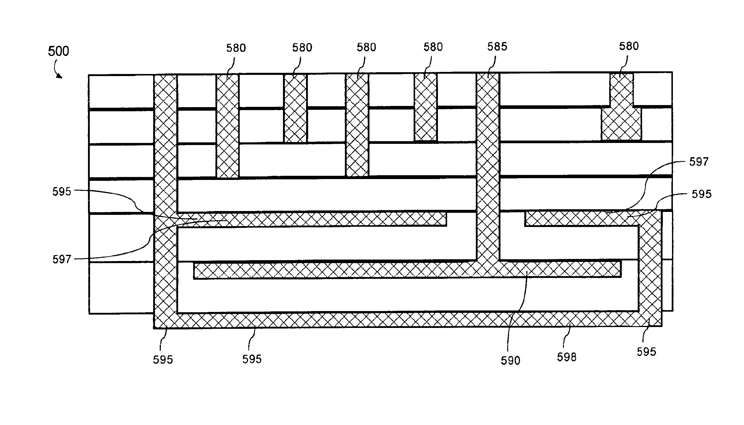
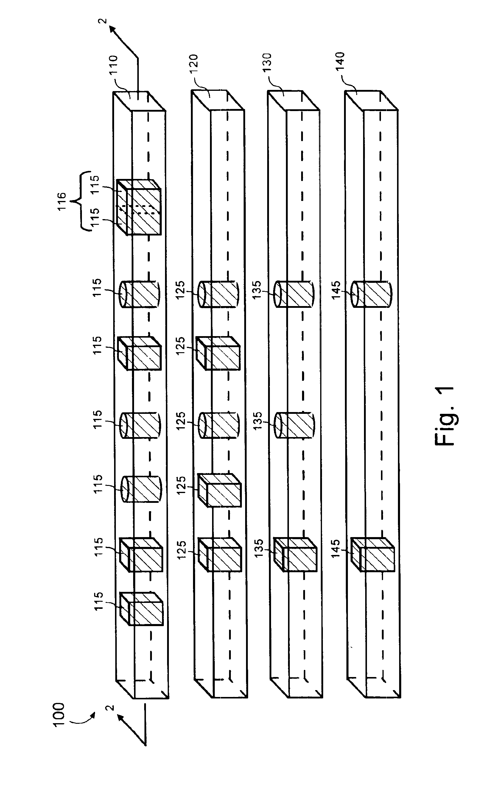
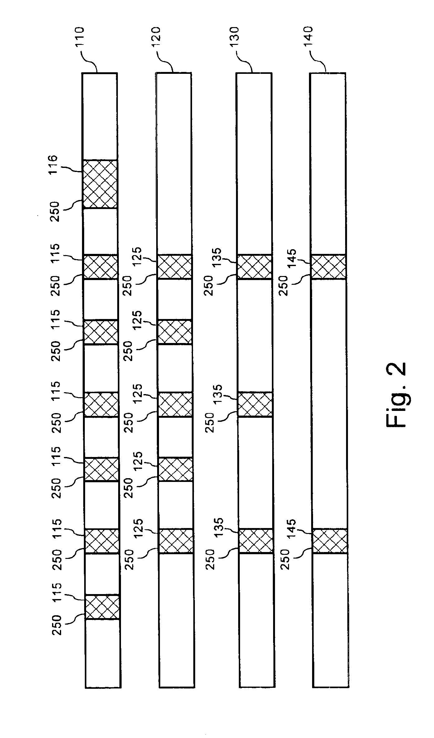
[0018]The present invention provides a substrate having embedded capacitors formed therein. Notably, since the capacitors are formed within the substrate, a greater amount of substrate surface area is available for positioning of other components. Moreover, the size of a substrate can be reduced since area that would normally be used by surface mounted capacitors is no longer required.

[0019]The substrate can include one or more dielectric layers. Vias, or bores, can be provided in the dielectric layers. The vias can be filled with conductive material to form electrodes. A capacitor can be formed by an electrode, another conductor not electrically shorted to the electrode, and the dielectric material disposed between the electrode and other conductor. The amount of dielectric material disposed between the electrode and the other conductor can be controlled by selecting the depth of the electrode within the substrate. For example, the electrode can extend through a single dielectric l...


PUM


Abstract

Embedded capacitors and a method for manufacturing the embedded capacitors. The method can include the steps of forming at least one bore (115) in a dielectric substrate (100). The dielectric substrate can be mechanically punched or laser cut to form the bore. The bore can be filled with a conductive material (250) to form a first electrode (470). A conductor (360) can be formed on the dielectric substrate, the conductor not being electrically continuous with the first electrode. A depth and / or cross sectional area of the bore can be selected to provide a desired amount of capacitive coupling between the electrode and the conductor. At least a second bore can be formed in the dielectric substrate and filled with a conductive material to form a second electrode. The second electrode can be electrically connected to the first electrode.

Description

BACKGROUND OF THE INVENTION[0001]1. Statement of the Technical Field[0002]The inventive arrangements relate generally to the field of capacitors, and more particularly to capacitors embedded in a substrate.[0003]2. Description of the Related Art[0004]Embedded capacitors are currently available in both printed wire board (PWB) and low temperature co-fired ceramic (LTCC) technologies. Typically, printed conductors are deposited on a substrate and used as electrodes for a capacitor. In some instances, the substrate itself can serve as the dielectric for the capacitor. In other arrangements, a via within the substrate can be filled with a dielectric material.[0005]Using LTCC, the printed conductors are typically created using a printed thick film process. Etching processes are typically used for PWB's. In either case, forming capacitors with tight tolerances can be difficult. In particular, it is often difficult to precisely control the area of the electrode. A small difference in elect...

Claims


Application Information

Patent Timeline
IPC IPC(8): H01L21/70H01L21/8242H01P3/02H01P3/06H01G4/20H01G4/26H01L21/425H01L21/4763H01L23/498H05K1/16H05K3/40H05K3/46
CPCH01L23/49822H05K1/162H01L2924/09701H05K1/0239H05K3/4061H05K3/4069H01L2924/0002H05K3/4614H05K2201/096H05K2201/09672H01L2924/00H01G4/26H10B99/00
Inventor PROVO, TERRY M.THOMSON, ANDREW J.
Owner HARRIS CORP
Features
  • R&D
  • Intellectual Property
  • Life Sciences
  • Materials
  • Tech Scout
  • Unparalleled Data Quality
  • Higher Quality Content
  • 60% Fewer Hallucinations
Learn More