Techniques for making a circuit board with improved impedance characteristics

a technology of impedance characteristics and circuit boards, which is applied in the direction of printed circuit aspects, circuit electrical arrangements, high frequency circuit adaptations, etc., can solve the problems of preventing circuit board manufacturers from modifying particular aspects of signal layer traces, and manufacturers may not be able to make differential pair traces of 150 ohms slightly narrower, so as to defeat the purpose of providing differential signal differential traces

Inactive Publication Date: 2005-06-21
EMC IP HLDG CO LLC
View PDF6 Cites 16 Cited by
  • Summary
  • Abstract
  • Description
  • Claims
  • Application Information

AI Technical Summary

Problems solved by technology

Unfortunately, there are deficiencies to the above-described conventional approach to designing a circuit board having a signal layer which includes differential pair traces of different impedance values.
In particular, limitations may exist that prevent the circuit board manufacturer from modifying particular aspects of the signal layer traces.
However, the manufacturer may not be able to make the differential pair traces of 150 Ohms slightly narrower if the manufacturer has already set the 100 Ohm differential pair traces to the minimum trace width acceptable for the circuit board.
Making a trace narrower than the minimum trace width acceptable for the circuit board would result in the manufacturer violating the circuit board specifications and perhaps lead to undesirable side effects (e.g., improper signal strength, timing anomalies, open circuits, capacitance problems, etc.).
Furthermore, the manufacturer may not wish to increase the trace separation distance between the differential pair traces since such an increase in separation could result in exposing the data signals within the differential pair traces to different interference patterns thus defeating the purpose of providing the differential pair traces for differential signals, i.e., the data signals within the differential pair traces may no longer share the same noise.

Method used


Image

  • Techniques for making a circuit board with improved impedance characteristics
  • Techniques for making a circuit board with improved impedance characteristics
  • Techniques for making a circuit board with improved impedance characteristics

Examples


Embodiment Construction

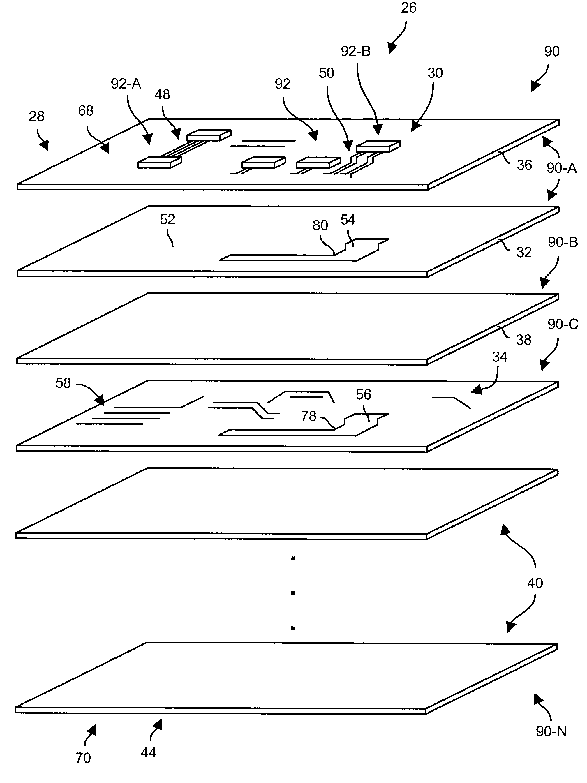
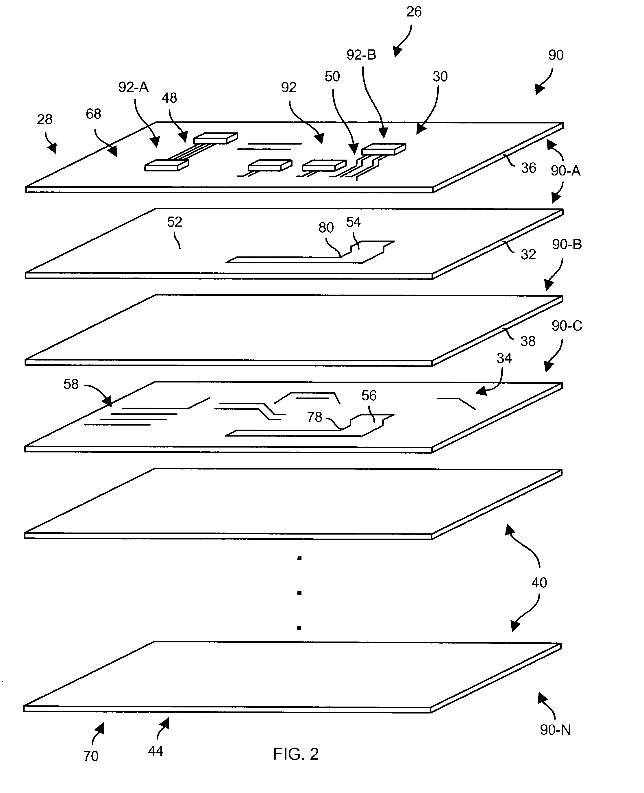
[0022]The invention is directed to techniques for making a circuit board which involve, relative to a set of signal layer traces, placing a non-conductive region within a conductive plane of another signal layer, and a mirroring conductive region in yet another signal layer. Accordingly, any signal layer trace passing over the non-conductive region within the conductive plane can derive its impedance based on its distance from the mirroring conductive region rather than its distance from the conductive plane. As a result, some signal layer traces can have a first impedance based on distance from the conductive plane while other signal layer traces can have a second impedance, which is different than the first impedance, based on distance from the conductive region.

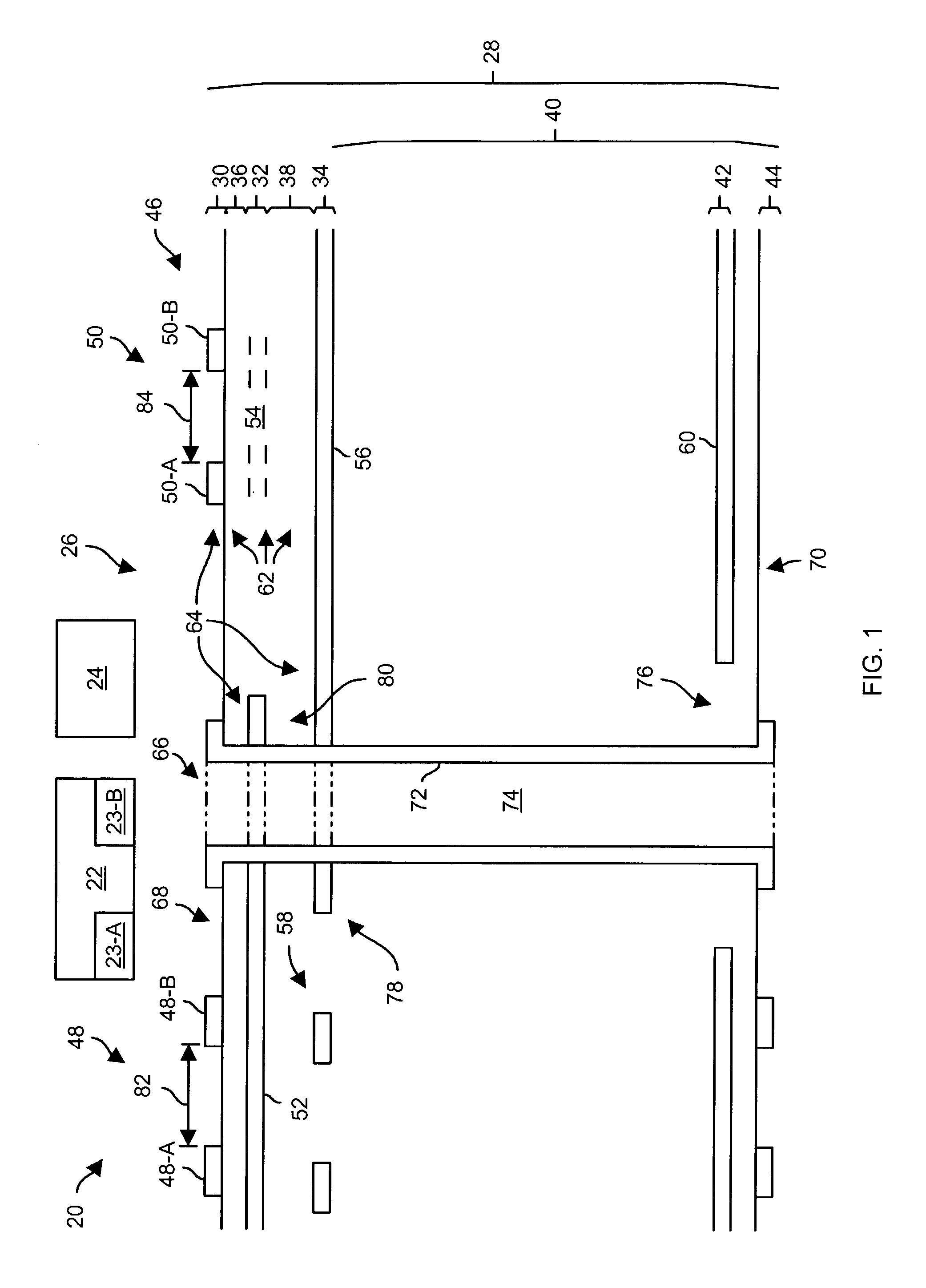
[0023]FIG. 1 shows an electronic system 20 which is suitable for use by the invention. The electronic system 20 includes a power supply 22 having a voltage terminal 23-A and a ground terminal 23-B. The electronic system 20...


PUM


Abstract

A circuit board has a first signal layer having a set of conductors, a second signal layer having a conductive plane and a non-conductive region, and a third signal layer having a conductive region that mirrors the non-conductive region of the second signal layer. The circuit board further includes a first separating layer having non-conductive material which is disposed between the first signal layer and the second signal layer, and a second separating layer having non-conductive material which is disposed between the second signal layer and the third signal layer. Accordingly, traces within the first signal layer and overlying the conductive plane of the second signal layer will have a first impedance, while traces within the first signal layer and overlying the non-conductive region of the second signal layer and the conductive region of the third signal layer will have a second impedance that is different than the first impedance.

Description

BACKGROUND OF THE INVENTION[0001]A typical circuit board includes layers of conductive material (e.g., copper) and non-conductive material (e.g., fiberglass) sandwiched together to form a single, rigid board. Some circuit boards include many layers (e.g., more than 20 layers of material).[0002]In general, to manufacture a circuit board having many layers, a circuit board manufacturer creates separate circuit board sheets. Each circuit board sheet typically includes two conductive signal layers and a non-conductive separating layer disposed between the conductive signal layers. The manufacturer typically aligns the circuit board sheets on top of each other and along with other non-conductive sheets (e.g., non-conductive core layers) in an interleaved manner, and laminates the sheets together to form an integrated board, e.g., applies glue, pressure and heat to combine the sheets into the board. Then, among other things, the manufacturer cuts and drills particular features into the bo...

Claims


Application Information

Patent Timeline
Patent Type & Authority Patents(United States)
IPC IPC(8): H05K1/00H05K1/02H05K7/06
CPCH05K1/025H05K1/0224H05K1/0245H05K1/0253H05K1/0298H05K2201/093H05K2201/09336H05K2201/0969H05K2201/09781
Inventor HAUG, DARRIN J.BARNEY, BRANDON
Owner EMC IP HLDG CO LLC
Why Eureka
Try Eureka