Method for fabricating microelectronic fabrication electrical test apparatus electrical probe tip having pointed tips

Inactive Publication Date: 2005-06-21
TAIWAN SEMICON MFG CO LTD
View PDF8 Cites 59 Cited by
  • Summary
  • Abstract
  • Description
  • Claims
  • Application Information

AI Technical Summary

Benefits of technology

[0020]The present invention provides an electrical test apparatus for electrically testing a microelectronic fabrication, wherein the microelectronic fabrication is tested with enhanced accuracy.
[0021]The present invention realizes the foregoing object with respect to an electrical probe tip employed within the electrical test apparatus, by fabricating the electrical probe tip (with enhanced precision) with a high density plasma chemical vapor deposition (HDP-CVD) deposited mandrel layer having formed therein (with enhanced precision) a series of pointed tips, such that a conductor probe tip layer formed conformally upon the high density plasma chemical vapor deposition (HDP-CVD) deposited mandrel layer replicates the series of pointed tips. In turn the series of replicated pointed tips provides for enhanced contact and enhanced accuracy when electrically testing a microelectronic fabrication while employing an electrica

Problems solved by technology

While electrical testing of microelectronic fabrications to assure proper and functional operation of microelectronic fabrications is common in the art of microelectronic fabrication, electrical testing of microelectronic fabrications to assure proper and functional operation of microelectronic fabrications is nonetheless not entirely without problems in the art of microelectronic fabrication.
In that regard, it is often difficult in the art of microelectronic fabrication when electrical probe tip contact testing microelectronic fabrications within the art of microelectronic fabricati

Method used


Image

  • Method for fabricating microelectronic fabrication electrical test apparatus electrical probe tip having pointed tips
  • Method for fabricating microelectronic fabrication electrical test apparatus electrical probe tip having pointed tips
  • Method for fabricating microelectronic fabrication electrical test apparatus electrical probe tip having pointed tips

Examples


Embodiment Construction

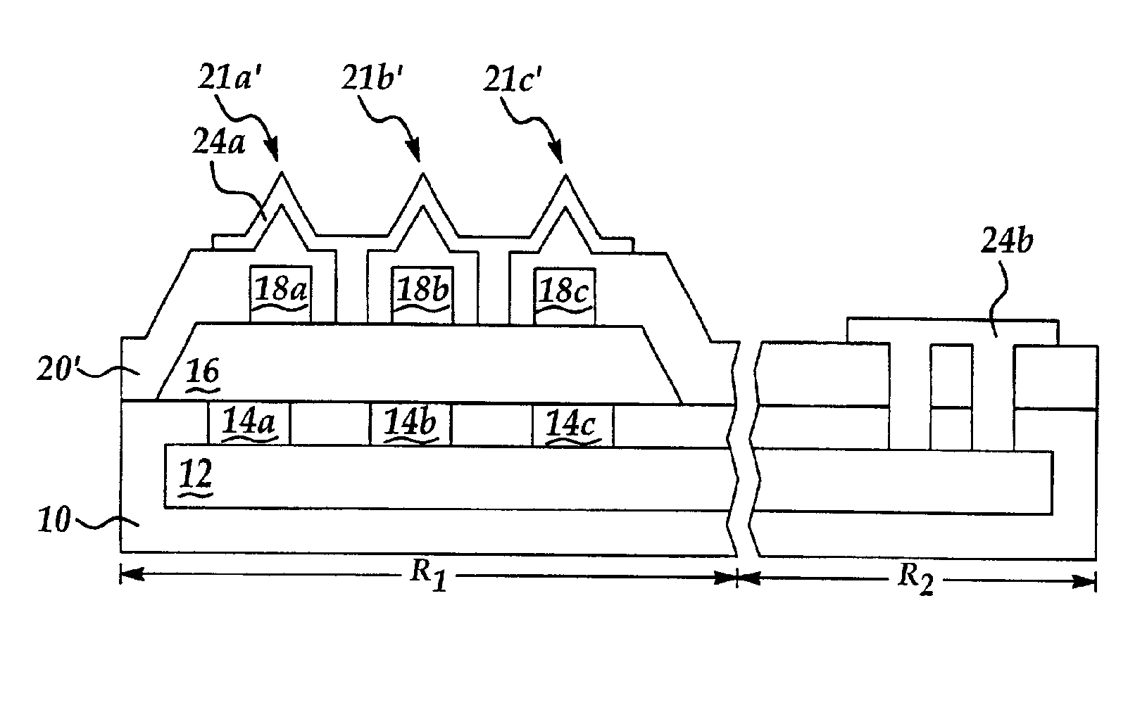
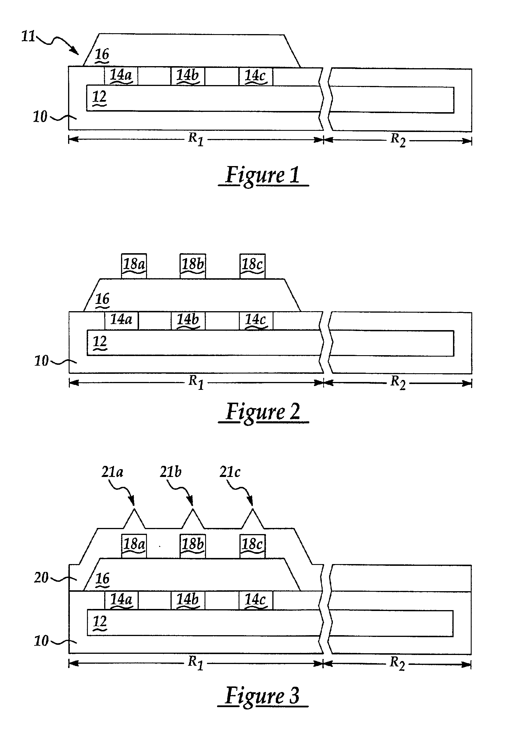
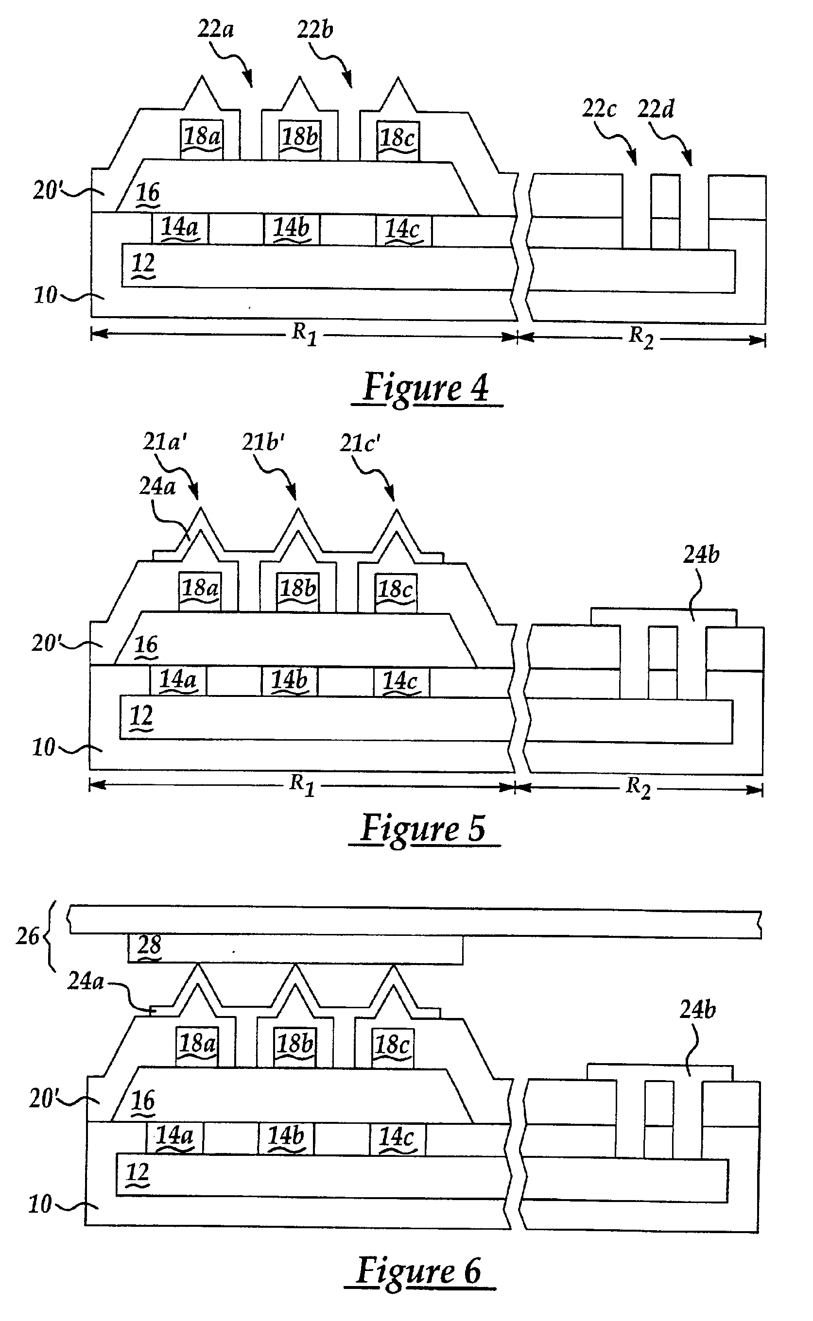
[0027]The present invention provides an electrical test apparatus for electrically testing a microelectronic fabrication, wherein the microelectronic fabrication is tested with enhanced accuracy.

[0028]The present invention realizes the foregoing object with respect to an electrical probe tip employed within the electrical test apparatus, by fabricating the electrical probe tip with a high density plasma chemical vapor deposition (HDP-CVD) deposited mandrel layer having formed therein a series of pointed tips, such that a conductor probe tip layer formed upon the high density plasma chemical vapor deposition (HDP-CVD) deposited mandrel layer replicates the series of pointed tips. In turn the series of replicated pointed tips provides for enhanced contact and enhanced accuracy when electrically testing a microelectronic fabrication while employing an electrical test apparatus having assembled therein the electrical probe tip.

[0029]Referring now to FIG. 1 to FIG. 5, there is shown a se...


PUM


Abstract

A method for fabricating an electrical test apparatus electrical probe tip first provides a probe tip substrate having a topographic surface. A high density plasma chemical vapor deposition (HDP-CVD) deposited mandrel layer is then formed upon the topographic surface. It has a series of pointed tips formed over a series of topographic features within the topographic surface. Finally, a conductor probe tip layer is formed conformally upon the high density plasma chemical vapor deposition (HDP-CVD) deposited mandrel layer and replicating the series of pointed tips. Due to the series of pointed tips and the series of replicated pointed tips, a microelectronic fabrication when tested with the electrical test apparatus electrical probe tip is tested with enhanced accuracy.

Description

BACKGROUND OF THE INVENTION[0001]1. Field of the Invention[0002]The present invention relates generally to methods for fabricating microelectronic fabrication electrical test apparatus electrical probe tips. More particularly, the present invention relates to methods for fabricating, with enhanced efficiency, microelectronic fabrication electrical test apparatus electrical probe tips.[0003]2. Description of the Related Art[0004]Microelectronic fabrications are formed from microelectronic substrates over which are formed patterned microelectronic conductor layers which are separated by microelectronic dielectric layers.[0005]Incident to the fabrication of various types of microelectronic fabrications within the art of microelectronic fabrication, it is common in the art of microelectronic fabrication to electrically test microelectronic fabrications to assure proper and functional operation of the microelectronic fabrications.[0006]While electrical testing of microelectronic fabricat...

Claims


Application Information

Patent Timeline
IPC IPC(8): G01R1/067G01R3/00
CPCG01R1/06738G01R3/00
Inventor LU, NAI-CHENGLIAO, YU-TINGLIU, FU-SUNG
Owner TAIWAN SEMICON MFG CO LTD
Why Eureka
Try Eureka