Method of collecting impurities on surface of semiconductor wafer

Active Publication Date: 2005-06-28
RENESAS ELECTRONICS CORP
View PDF3 Cites 4 Cited by
  • Summary
  • Abstract
  • Description
  • Claims
  • Application Information

AI Technical Summary

Problems solved by technology

Particularly, when contamination due to metal impurities occurs, the increase of leakage current and the deterioration of withstand pressure are caused and the reliability of a device is largely damaged.
At this time, there is also a measuring method by total reflection fluorescent X-ray spectroscopy (TXRF) in which metal impurities are not required to be collected, however, as this method has an element such as Al and Na which cannot be analyzed or an element which is not satisfactory in sensitivity, a method of collecting and chemically analyzing is required.
However

Method used


Image

  • Method of collecting impurities on surface of semiconductor wafer
  • Method of collecting impurities on surface of semiconductor wafer
  • Method of collecting impurities on surface of semiconductor wafer

Examples


Embodiment Construction

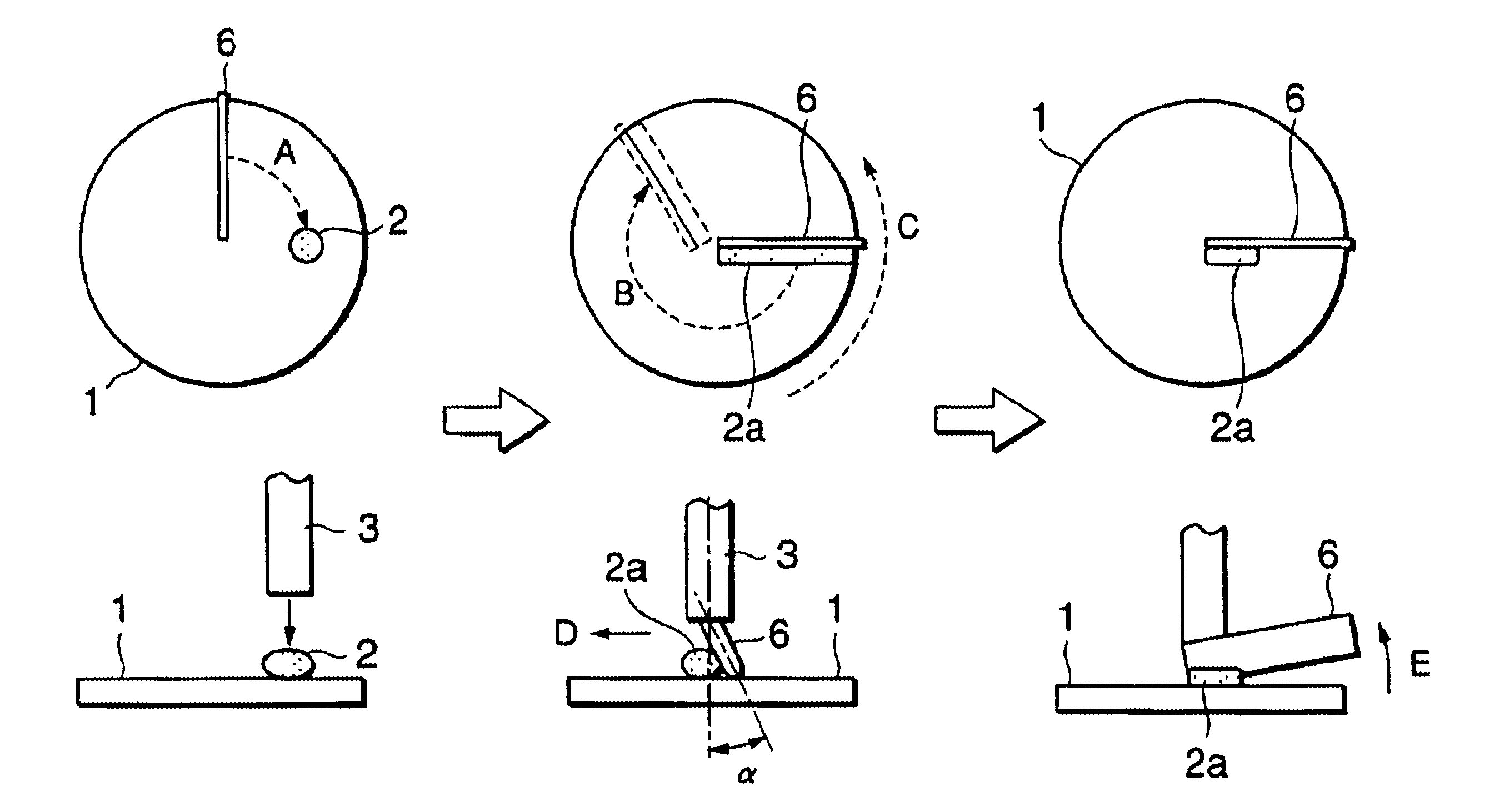
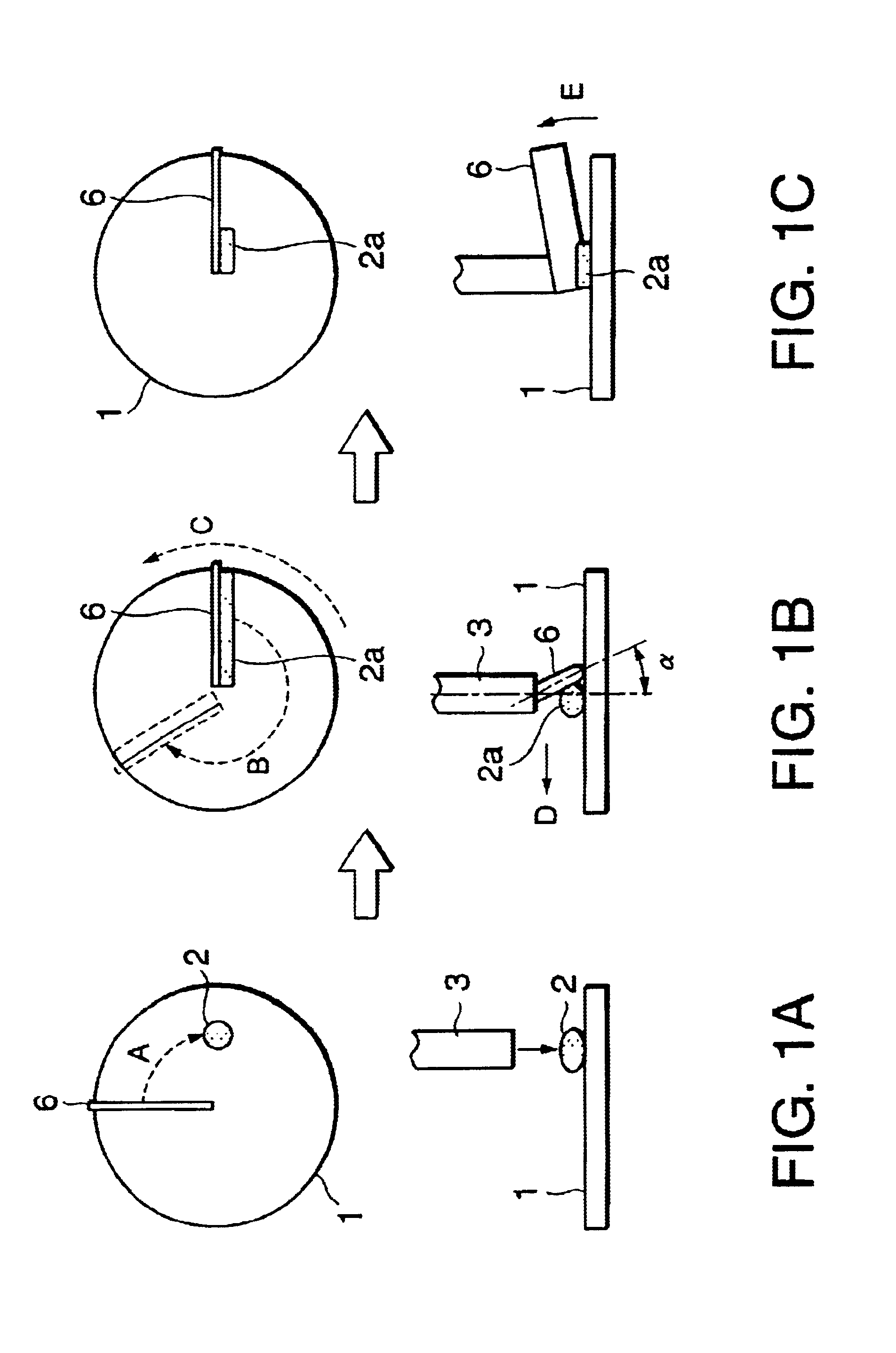
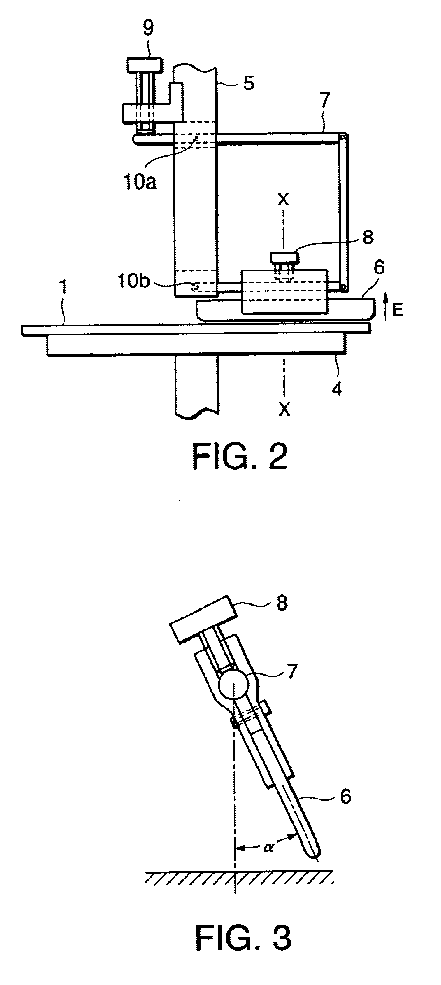
[0019]Next, referring to the drawings, an embodiment of the invention will be described. FIG. 2 is a front view showing the schematic structure of an apparatus for collecting impurities on the surface of a semiconductor wafer used in one embodiment of the invention and FIG. 3 is a sectional view viewed along a line X—X in FIG. 2.

[0020]As shown in FIG. 2, a rotating table 4 on which a semiconductor wafer 1 to be inspected is horizontally laid and is fixed by a vacuum chuck and which can be moved in directions of the x-, y- and z-axes, a vertical rotating shaft 5 installed above the rotating table 4 and a scanning plate 6 attached to a link mechanism 7 provided in a lower part of the vertical rotating shaft 5 are provided. The link mechanism 7 is attached to the vertical rotating shaft 5 at rotation supporting points 10a and 10b. The scanning plate 6 is formed so that the length is equivalent to the radius of the semiconductor wafer 1 or is slightly longer (for example, 155 mm in the ...


PUM

PropertyMeasurementUnit
Lengthaaaaaaaaaa
Shapeaaaaaaaaaa
Radiusaaaaaaaaaa

Abstract

A method of collecting impurities existing on the surface of a semiconductor wafer and in a thin film formed on the semiconductor wafer is provided with a process for dripping collecting liquid on the surface of the semiconductor wafer to which hydrophobic processing is applied, a process for elongating the collecting liquid dripped and turned spherical by surface tension in a direction of the radius of the semiconductor wafer with the surface tension kept, a process for relatively rolling and scanning the elongated collecting liquid, touching the collecting liquid to the surface of the semiconductor wafer and incorporating impurities into the collecting liquid, a process for restoring the elongated collecting liquid to the original spherical shape after the impurities are incorporated and a process for withdrawing the collecting liquid restored to the spherical shape from the surface of the semiconductor wafer.

Description

BACKGROUND OF THE INVENTION[0001]1. Field of the Invention[0002]The present invention relates to a method of collecting impurities on the surface of a semiconductor wafer for collecting a tiny amount of impurities existing on the surface of the semiconductor wafer and in a thin film formed on the semiconductor wafer and analyzing the impurities.[0003]2. Description of the Prior Art[0004]In a conventional type manufacturing process of a semiconductor wafer, it is required to advance a process, always monitoring a contaminated state of the surface of the semiconductor wafer. Particularly, when contamination due to metal impurities occurs, the increase of leakage current and the deterioration of withstand pressure are caused and the reliability of a device is largely damaged. Then, to investigate the extent of contamination, inspection that metal impurities are collected from the surface of a semiconductor wafer, are chemically analyzed and the type and quantity of the metal impurities...

Claims


Application Information

Patent Timeline
IPC IPC(8): C23G1/36C23G1/00C25F1/00H01L21/66B08B3/04B08B7/00H01L21/00H01L21/02
CPCB08B3/04B08B7/0014H01L21/67051H01L21/02054Y10S438/906
Inventor WATANABE, KAORI
Owner RENESAS ELECTRONICS CORP
Why Eureka
Try Eureka