Multiple contact vertical probe solution enabling Kelvin connection benefits for conductive bump probing

a vertical probe and multi-contact technology, applied in the field of probe cards, can solve problems such as reducing device yields, affecting test negative effects, and high contact resistance during bump probing to correctly validate the operation of the ad

Inactive Publication Date: 2005-06-28
TEXAS INSTR INC
View PDF2 Cites 62 Cited by
  • Summary
  • Abstract
  • Description
  • Claims
  • Application Information

AI Technical Summary

Benefits of technology

[0014]Objects and advantages of the invention will in part be obvious, and will in part appear hereinafter, and will be accomplished by the present invention which provides methods and apparatus for making electrical contact with an array of target tests or contact points, such as conductive balls or conductive bumps (including but not limited to solder balls or bumps) by a probe card testing apparatus. The apparatus comprises a support substrate made of a non-conductive material which has a working surface and a back side. A multiplicity of probes extend from a first end of each of the probes on the back side of the substrate through the substrate to a contact end intended to make contact with the conductive ball or conductive bump connections on an integrated circuit or other circuit. The contact ends of the multiplicity of conductive probes extend a selected distance beyond the working surface of the support substrate and terminate at a multiplicity of locations which are arranged accord...

Problems solved by technology

These contaminants create a thin insulating layer that makes it very difficult to achieve and maintain very low contact resistances between the probe needle and the bump, thus, negatively affects test results and ultimately reducing device yields.
Unfortunately, contact resistance during bump probing is often too high to correctly validate the operation of the ADC for these two parameters.
Further, the magnitude and stability of contact and circuit resistances during ...

Method used


Image

  • Multiple contact vertical probe solution enabling Kelvin connection benefits for conductive bump probing
  • Multiple contact vertical probe solution enabling Kelvin connection benefits for conductive bump probing
  • Multiple contact vertical probe solution enabling Kelvin connection benefits for conductive bump probing

Examples


Embodiment Construction

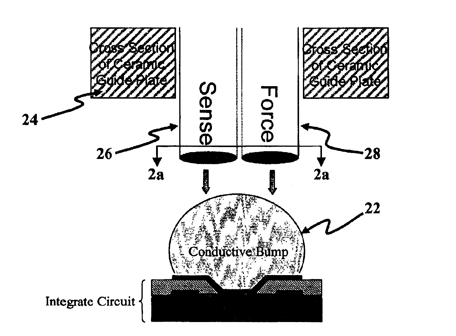
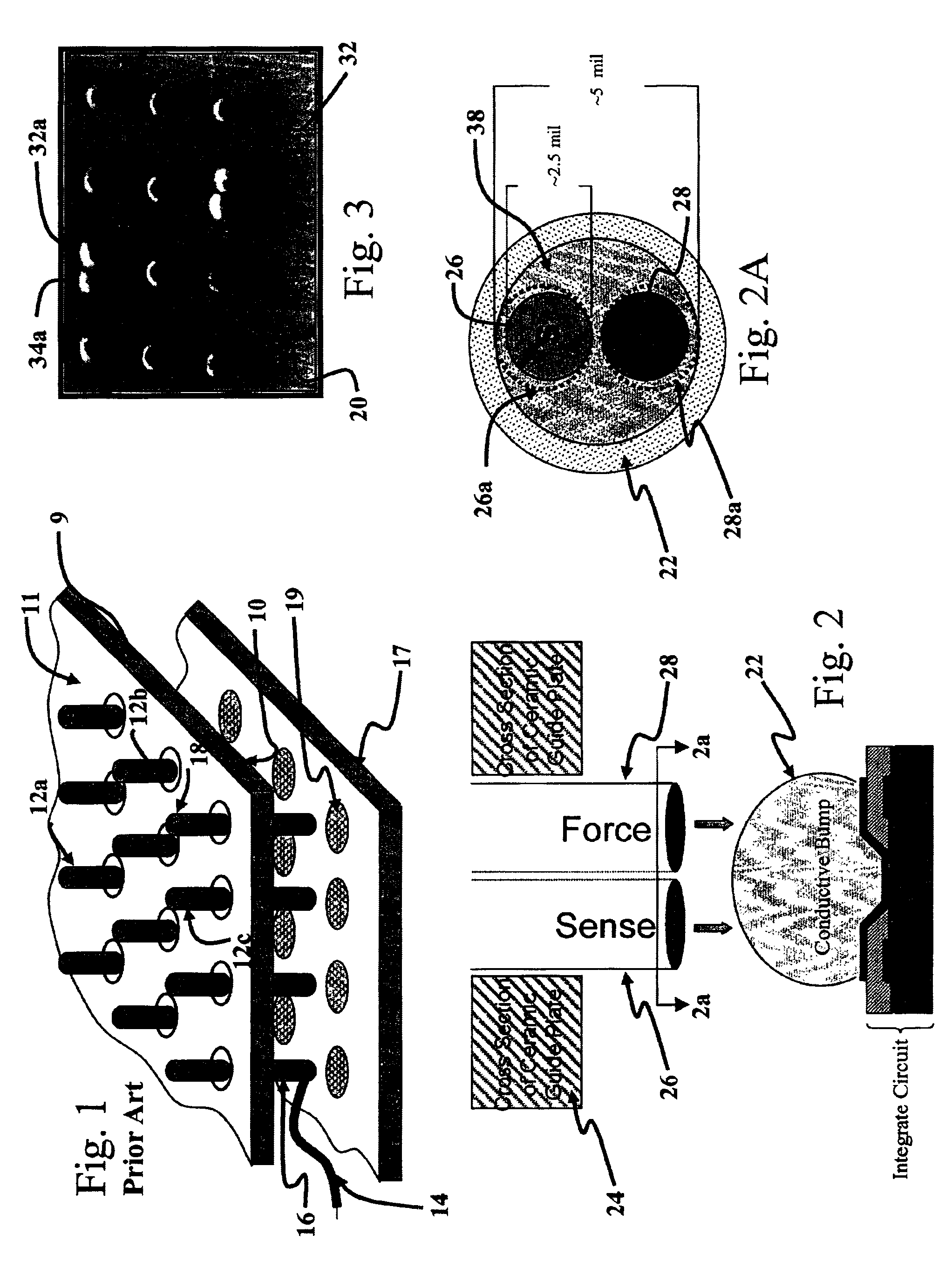
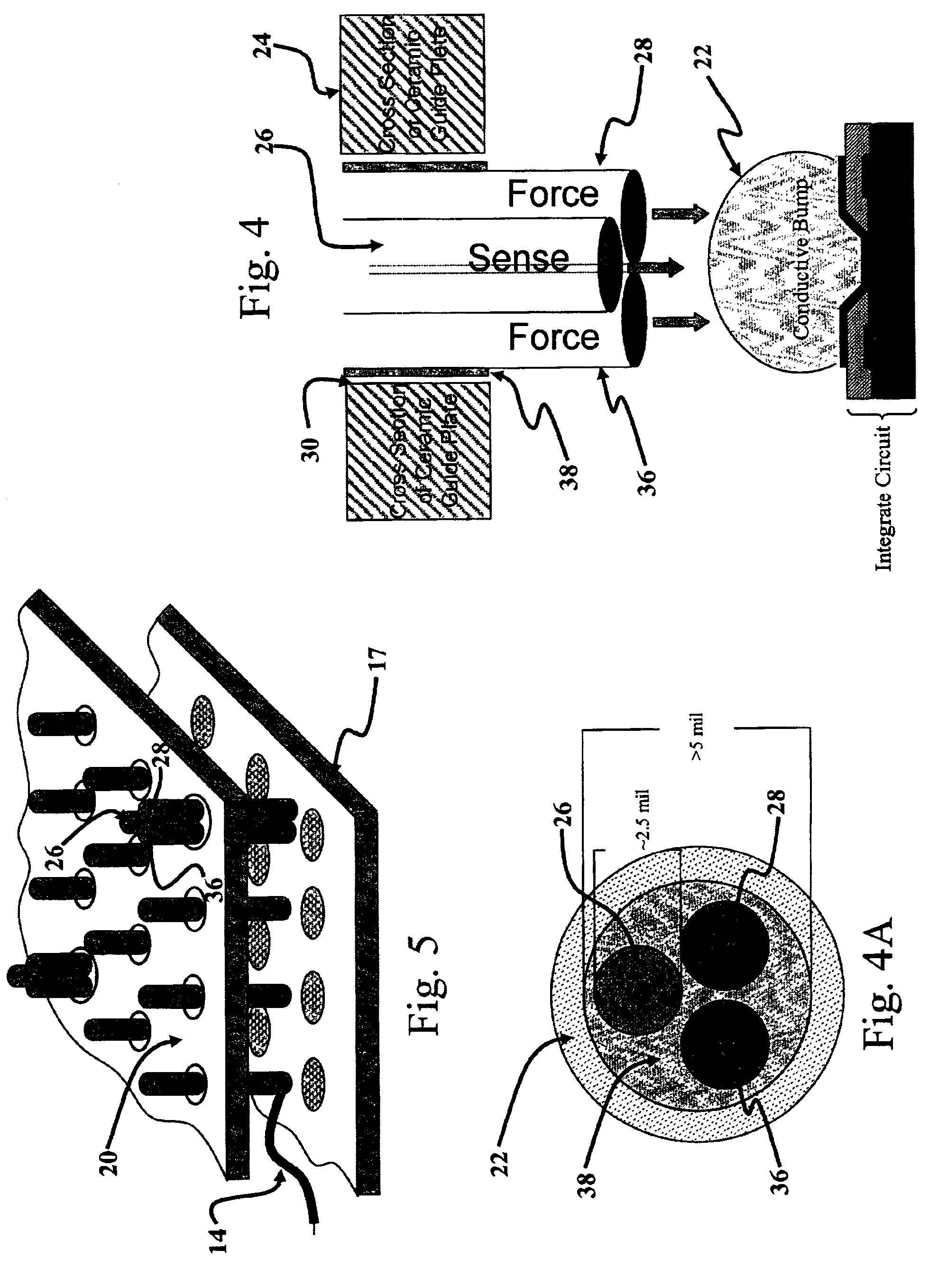
[0023]Referring now to FIG. 1, there is shown the bottom and partial perspective view of a prior art probe card using individual probes to contact each of the conductive ball contact or test points of a circuit being tested (such as for example, an IC or Integrated Circuit). It will be appreciated that the conductive ball contact points may include but are not limited to solder connections such as Lead-Tin, Silver and the like. As shown, the probe card typically comprises a non-conducting guide structure 10 which is typically planer and which guides a plurality of probes or probe tips (including probe tips 12a, 12b and 12c) which are arranged within the substrate 10 in a selected pattern which is a mirror image of the pattern or array of conductive ball or conductive bump contact points or test connections on a circuit to be tested.

[0024]The back end of each of the individual electrically conductive probes are connected to a conductive path such as a wire 14 connected to the back en...


PUM


Abstract

Apparatus and methods for testing conductive bumps or target test points on integrated circuits. A multiplicity of probes are extended through a support substrate. At least one of the multiplicity of probe locations include a second electrically isolated probe such that the test point is in contact with two probes. One of the two probes provides a voltage to the test point and the second probe sensing the voltage so as to provide a Kelvin connection.

Description

FIELD OF THE INVENTION[0001]This invention relates to testing of circuits (such as integrated circuits) having a large number of contact points such as conductive bumps or conductive balls. More specifically, the invention relates to a probe card used in such testing which minimizes the effect of IR voltage drops due to residue, oxide barriers and the like on the surface of such conductive ball connections. These surface contaminates create a thin insulative layer between the probe tips of a probe card and the conductive ball contact points or target test points.BACKGROUND OF THE INVENTION[0002]Probing on conductive bumps, or balls, during wafer level test to make an electrical connection to the integrated circuit (IC) device is typically accomplished during a single pass or contact between a probe card and the IC device. The conductive ball, or bump, application process is intrinsically unclean. In addition to the natural oxide barriers, there are residual organic materials that re...

Claims


Application Information

Patent Timeline
IPC IPC(8): G01R1/073
CPCG01R1/07314
Inventor MITCHELL, SCOTT W.RINCON, REYNALDO M.BROZ, JERRYLAUGIER, GERARD
Owner TEXAS INSTR INC
Why Eureka
Try Eureka