Diode-laser curing of liquid epoxide encapsulants

a technology of liquid epoxide and curing electrode, which is applied in the direction of railway components, nuclear engineering, non-metallic protective coating applications, etc., can solve the problems of unparallel mechanical strength, high oven cost, and unfavorable mechanical strength, and achieves high electrical-to-optical conversion efficiency and no effect on cure or mechanical strength of resin

Inactive Publication Date: 2005-07-05
COHERENT INC
View PDF20 Cites 13 Cited by
  • Summary
  • Abstract
  • Description
  • Claims
  • Application Information

AI Technical Summary

Benefits of technology

[0009]Preferably the light absorbing materials added to the thermally convertible liquid organic matrix are sufficiently light absorbing that at least 15 percent and more preferable about 70 percent or greater of the laser radiation can be absorbed by the liquid organic matrix layer. Further, the matrix should contain a sufficiently small percentage of the light absorbing materials so that the curing or mechanical strength of the resin is not affected by addition of the material. The laser radiation wavelength between about 600 and 1000 nm is selected because most basic thermally convertible liquid matrixes are intrinsically transparent (essentially non absorbing) at wavelengths in this range. This allows absorption of the laser radiation in the resin to be controlled by the above-discussed light-absorbing additive materials. Further, laser radiation in this wavelength can be generated by diode-lasers. Such lasers have a high electrical-to-optical conversion efficiency compared with other laser types.

Problems solved by technology

This is due to their unparalleled mechanical strength, adhesion properties and environmental stability, which combine to give excellent protection to electronic circuitry assembled on a PCB.
The requirement for oven-curing of the liquid epoxide encapsulants adds considerably to the cost of manufacturing “smart-cards”.
The ovens are expensive, occupy a relatively large volume of production space, for example, about 30 cubic meters (m3), and consume a relatively large amount of energy, for example, about 5 Kilowatts for an oven capable of curing 100 bonds per hour on cards having width of 75 millimeters (mm) and a length of 125 mm.
Further, the form of the ovens makes them unsuitable for integration into an electronic assembly line.

Method used


Image

  • Diode-laser curing of liquid epoxide encapsulants
  • Diode-laser curing of liquid epoxide encapsulants
  • Diode-laser curing of liquid epoxide encapsulants

Examples


Embodiment Construction

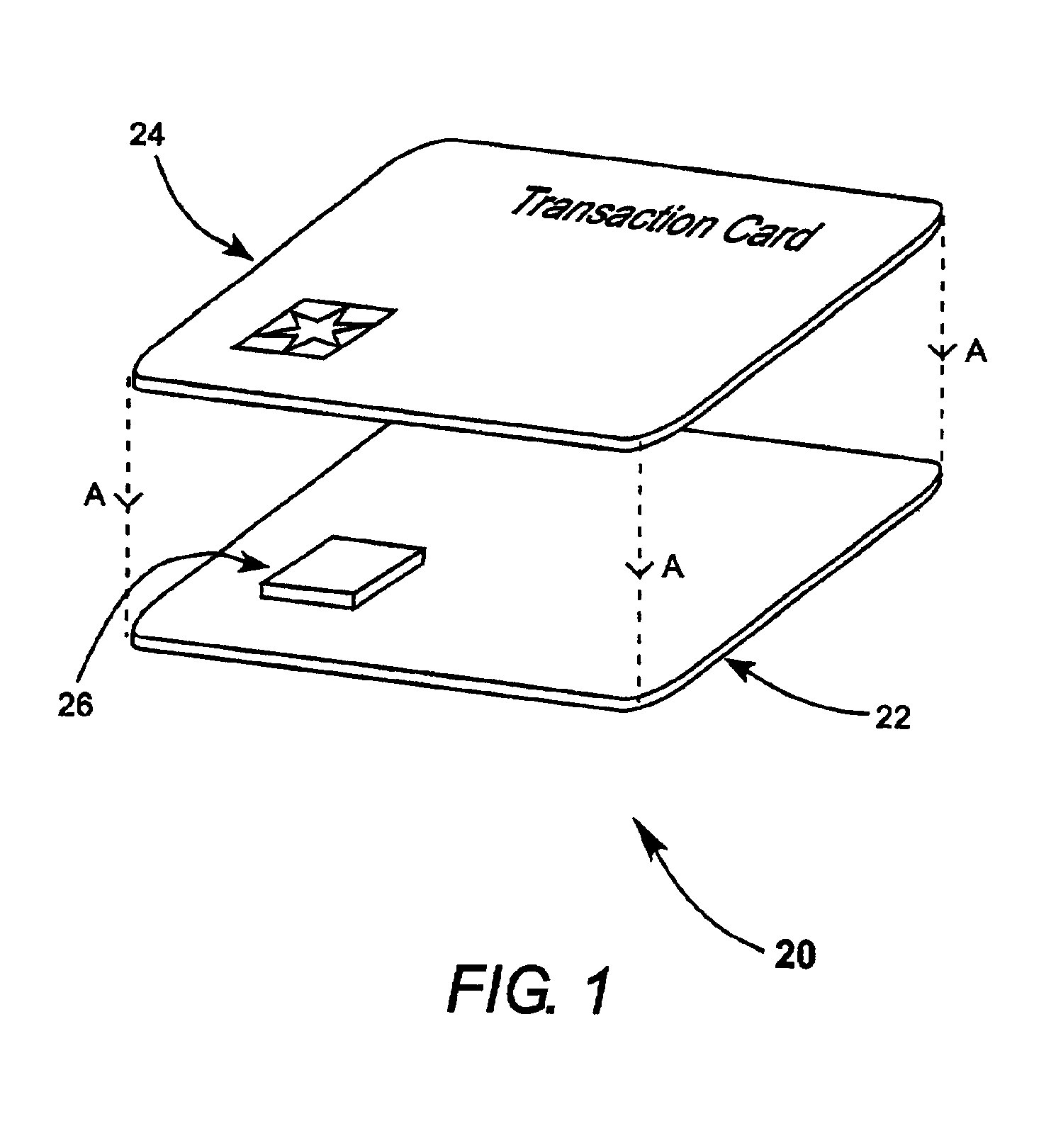
[0015]Referring now to the drawings, wherein like features are designated by like reference numerals, FIG. 1 schematically illustrates an example of a transaction card 20 having a substrate 22 with an IC chip 26 bonded thereon, and a cover 24. After IC chip 26 is bonded to substrate 22 and connected to other circuit components (not shown) the IC chip is encapsulated by the organic liquid matrix conversion method of the present invention and a cover 24 is laminated to substrate 22.

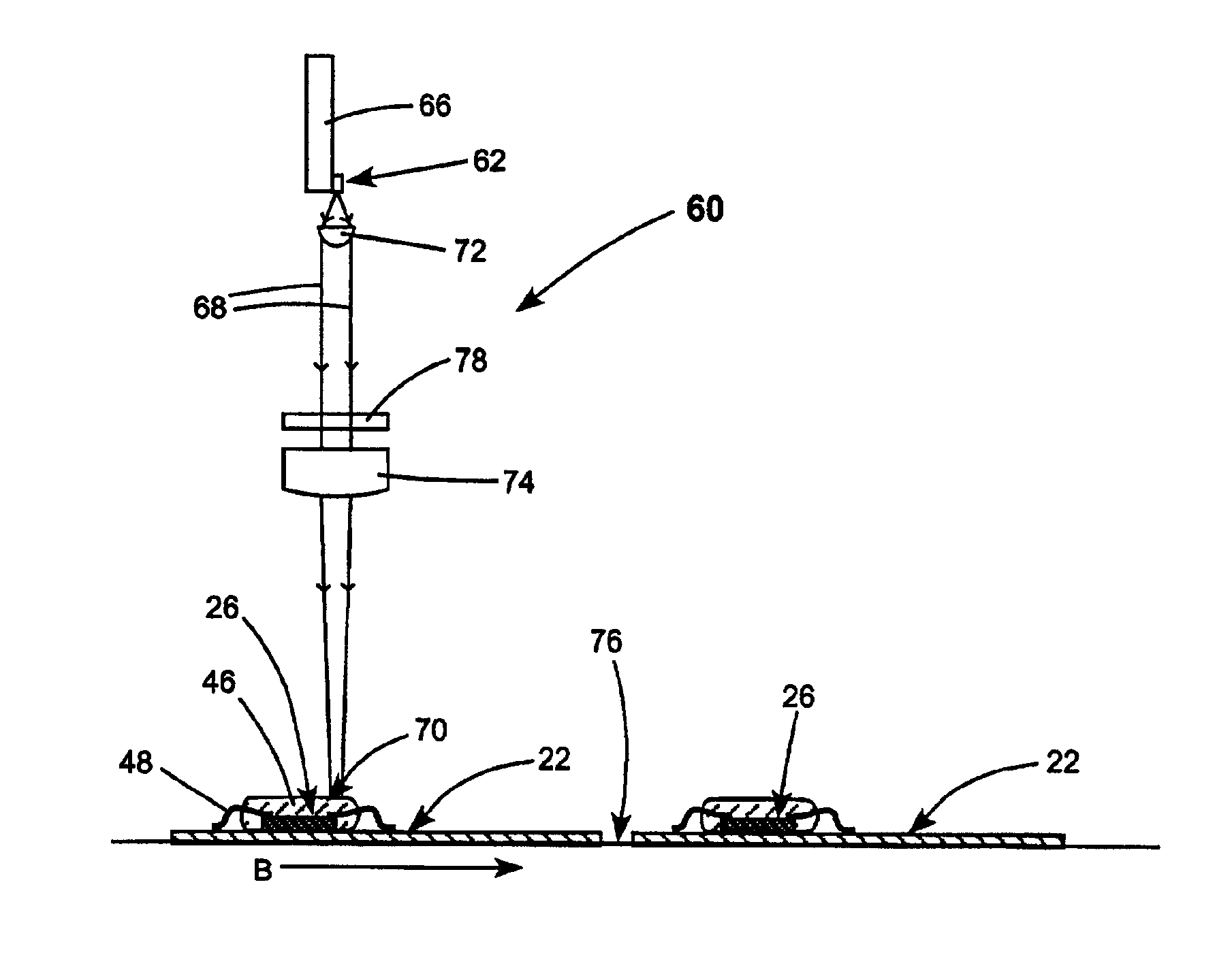
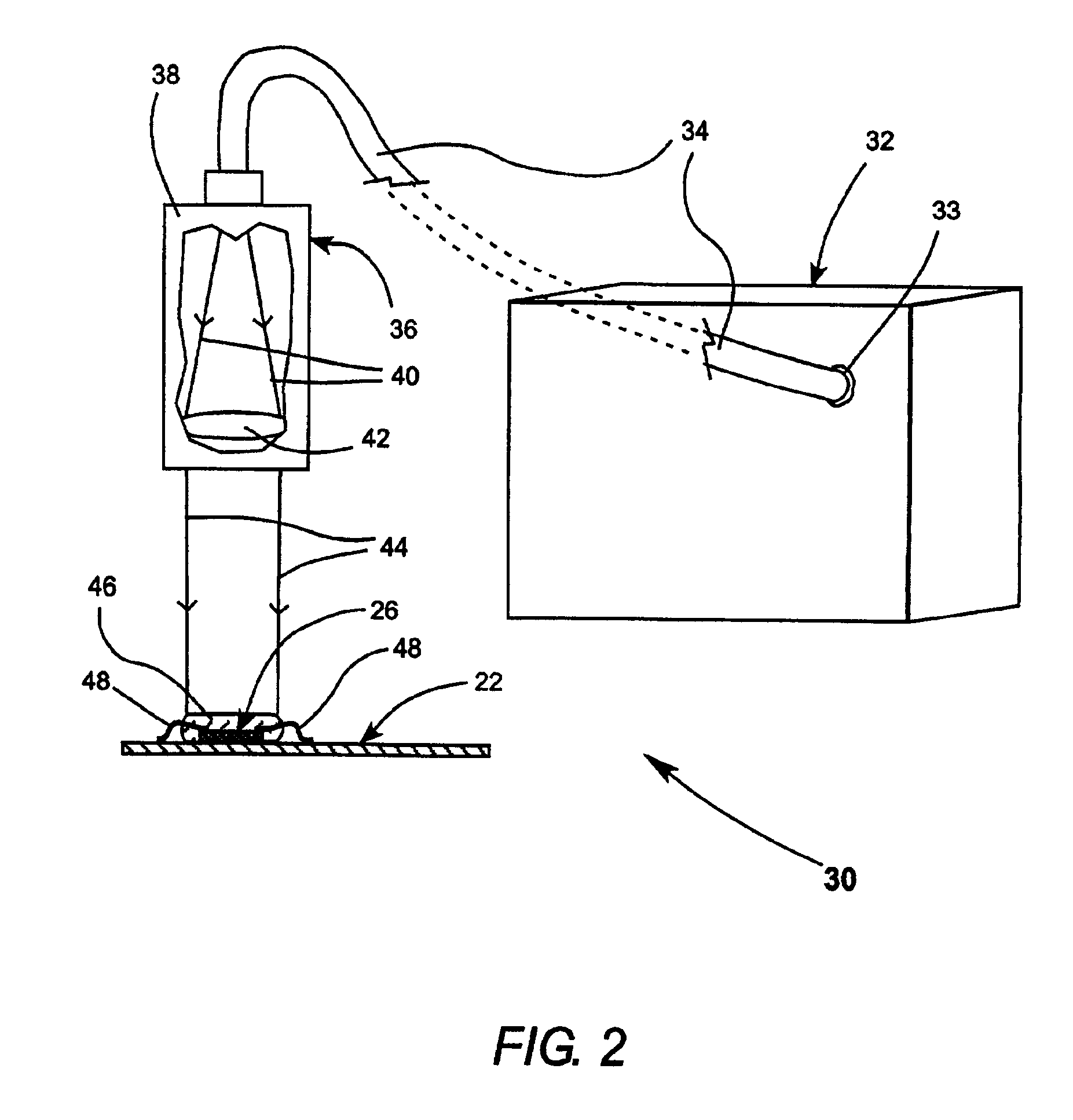
[0016]FIG. 2 depicts an example of apparatus 30 arranged for carrying out a preferred embodiment of the present invention for encapsulating IC chip 26 on a substrate 22. Apparatus 30 includes a diode-laser unit 32. Diode-laser unit 32 includes a high-power diode-laser array or diode-laser bar (not shown) the output of which is delivered to an optical-fiber connector 33. One suitable diode-laser unit capable of delivering up to 30 Watts (W) of diode-laser radiation is a FAP™ system available from Coherent®, ...


PUM

PropertyMeasurementUnit
wavelengthaaaaaaaaaa

Abstract

A method of encapsulating an integrated-circuit component supported on a substrate comprises depositing on the component a thermally curable liquid organic matrix in sufficient quantity to form a layer covering the component. The liquid matrix layer is irradiated by laser radiation having a wavelength between about 600 and 1000 nanometers. The liquid matrix includes one or more additive materials that are strongly absorbing for the wavelength of the laser radiation. The liquid matrix layer is irradiated with the laser radiation for a time period sufficient to cure the matrix layer.

Description

TECHNICAL FIELD OF THE INVENTION[0001]The present invention relates generally to thermally convertible liquid organic matrixes, such as formulated liquid epoxide encapsulants, adhesives and coating compounds. The invention relates in particular to converting (curing) such a liquid matrix by exposing the liquid matrix to laser radiation having a wavelength between about 660 and 1000 nm.DISCUSSION OF BACKGROUND ART[0002]Thermally converted formulated liquid epoxide encapsulants, adhesives and coating compounds are extensively used within the electronics industry for bonding and encapsulating integrated circuit (IC), diode, and other microelectronic packages to printed circuit boards (PCBs). This is due to their unparalleled mechanical strength, adhesion properties and environmental stability, which combine to give excellent protection to electronic circuitry assembled on a PCB. Such liquid epoxide adhesives and encapsulants, also widely known in the industry as “glob-top” or chip-on-b...

Claims


Application Information

Patent Timeline
Patent Type & Authority Patents(United States)
IPC IPC(8): B29C35/08B29C35/02H01L21/56G06K19/077H01L21/02H05K3/28
CPCB29C35/0272B29C35/0805G06K19/07745H01L21/56B29C33/06B29C2035/0838B29K2105/16H01L2224/8592H05K3/284H01L2224/48091H01L2224/48472H01L2924/00014H01L2924/00
Inventor HOULT, ANTHONY P.CRANE, SCOTT J.
Owner COHERENT INC
Why Eureka
Try Eureka