Double diffusion MOSFET with N+ and P+ type regions at an equal potential

a double diffusion mosfet and p+ technology, applied in semiconductor devices, semiconductor/solid-state device details, electrical apparatus, etc., can solve the problems of large igbt defect, easy breakage of devices, and large current of igbt processing, etc., to achieve the effect of easy adjustmen

Inactive Publication Date: 2005-07-05
ROHM CO LTD
View PDF4 Cites 21 Cited by
  • Summary
  • Abstract
  • Description
  • Claims
  • Application Information

AI Technical Summary

Benefits of technology

[0034]In the thus arranged semiconductor device, the breakdown withstand voltage of the L-DMOSFET may easily be adjusted by varying the drift length of the L-DMOSFET to be integrated toge

Problems solved by technology

And the device will easily be broken.
When an excessive current as by the static electricity flows through the IGBT, the parasitic thyristor is turned on, and the IGBT can process large current with extremely low operating resistance value.
This also is recognized as a large defect of the IGBT.
As described above, the conventional L-DMOSFET is advantageous in that it is easy to attain a high voltage sta

Method used


Image

  • Double diffusion MOSFET with N+ and P+ type regions at an equal potential
  • Double diffusion MOSFET with N+ and P+ type regions at an equal potential
  • Double diffusion MOSFET with N+ and P+ type regions at an equal potential

Examples


Embodiment Construction

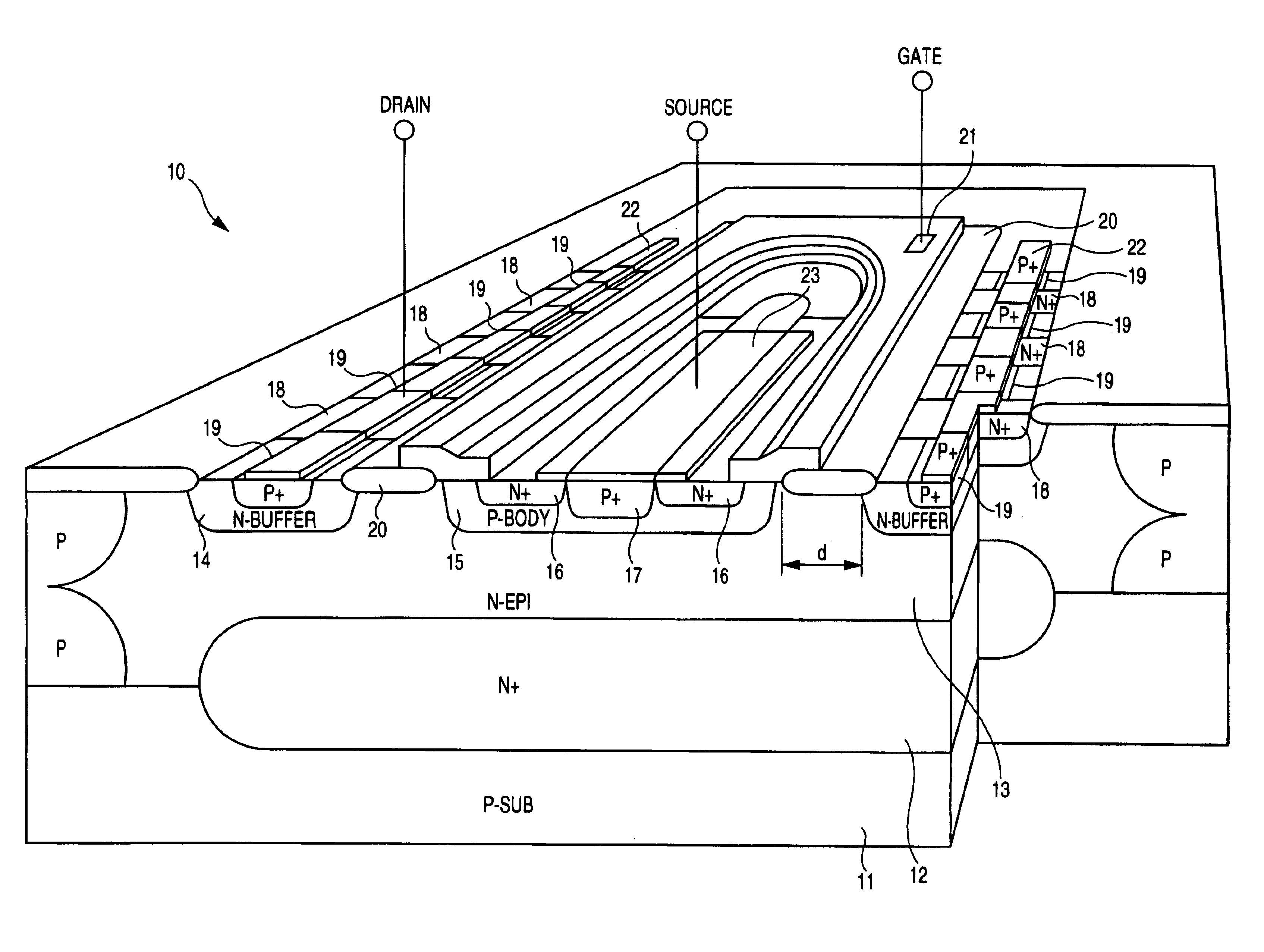
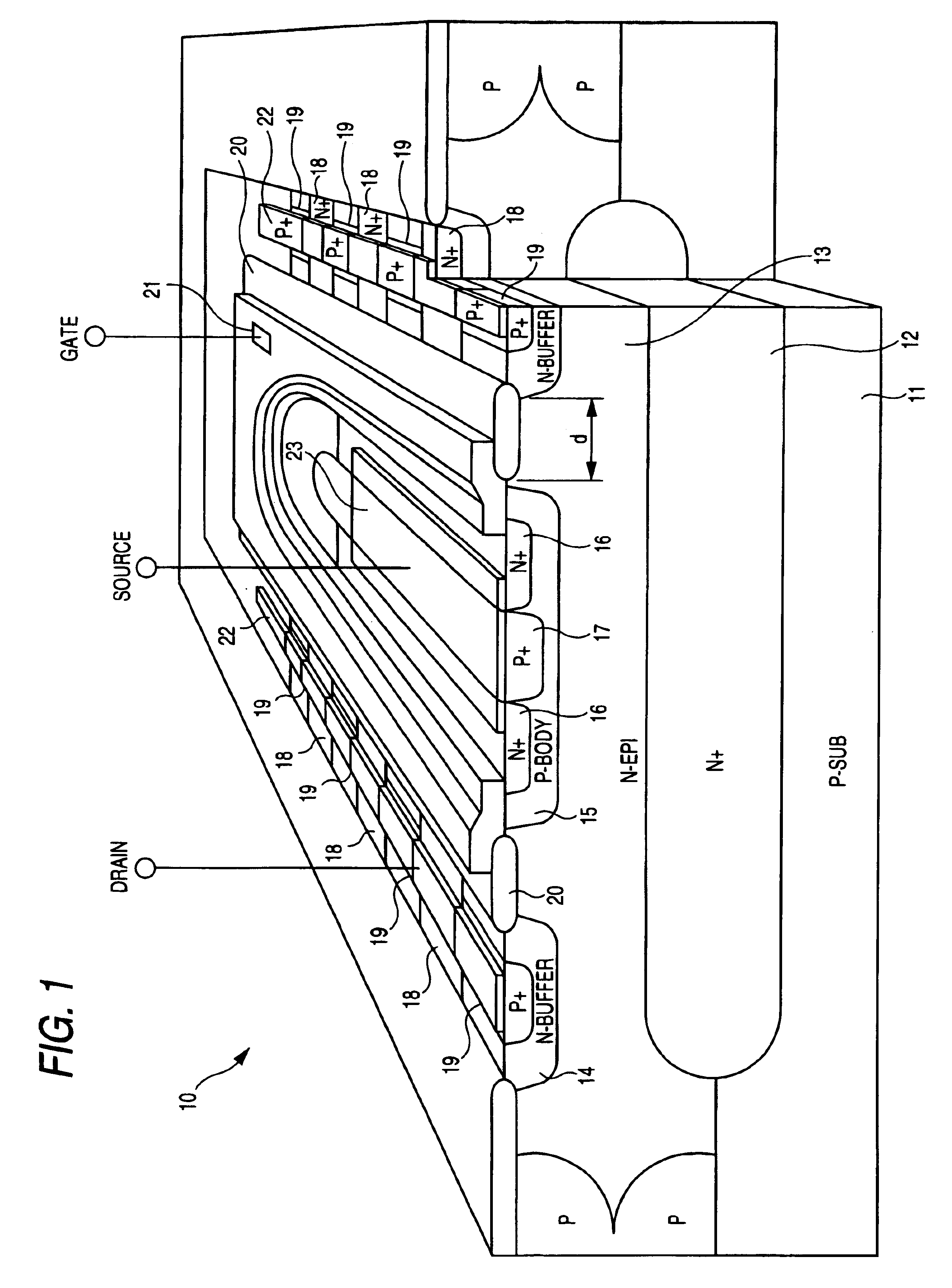
[0043]An L-DMOSFET constructed according to the present invention will be described with reference to the accompanying drawings.

[0044]FIG. 1 is a cross sectional view perspectively showing a double diffusion MOSFET which is an embodiment of the invention. A drain region 13 is formed in a manner that an N-type semiconductor layer is epitaxially grown on a P-type semiconductor substrate 11 with an N+ type buried region 12 being interposed therebetween. An N buffer layer 14 is formed by diffusing an N-type impurity into the drain region 13. A body region 15 is formed by diffusing a P-type impurity into the same.

[0045]An N+-type source region 16 is formed in a surface region of the body region 15, while being spaced apart from an outer edge of the body region 15. A P+-type region 17 is formed on the inner side of the N+-type source region 16. Within the N buffer layer 14, N+ type drain contact regions 18 and P+ type regions 19, while being in contact with one another are alternately arr...


PUM


Abstract

A double diffusion MOSFET is disclosed which comprises: a drain region 13 of an N-type semiconductor layer formed on a semiconductor substrate 11; a body region 15 of a P-type semiconductor region formed in the drain region 13; an N-type source region 16 formed in the body region 15; and a gate electrode 21 formed on a surface of the body region 15, wherein the drain region 13 contains N+ type drain contact regions 18 and P+ type regions 19 such that those are put at an equal potential.

Description

BACKGROUND OF THE INVENTION[0001]1. Field of the Invention[0002]The present invention relates to a lateral double diffusion MOSFET and a semiconductor device using the same, and more particularly to a lateral double diffusion MOSFET having a high Electro-static discharge performance (ESD) and low on-resistance.[0003]2. Description of the Related Art[0004]Lateral double diffusion MOSFETs, called L-DMOSs, are known for the FETs of ICs and discrete devices, which are generally used in a relatively low voltage region of 100V or lower. The lateral double diffusion MOSFET may be formed by normal diffusion process, and unlike the vertical double diffusion MOSFET, allows all the terminals to be drawn out from the chip top surface. Therefore, it is fit for use in IC fabrication, and is widely used where low on-resistance is required. FIG. 5 is a cross sectional view perspectively showing a conventional lateral double diffusion MOSFET. In the lateral double diffusion MOSFET (referred to as an...

Claims


Application Information

Patent Timeline
IPC IPC(8): H01L29/739H01L29/66H01L29/06H01L29/78H01L29/08H01L29/02H01L29/423
CPCH01L29/0878H01L29/42368H01L29/7393H01L29/7817H01L29/0696H01L29/0834H01L2924/0002H01L2924/00
Inventor HAMAZAWA, YASUSHI
Owner ROHM CO LTD
Why Eureka
Try Eureka