Method for measuring resistivity of semiconductor wafer

a technology of resistivity and semiconductor wafers, applied in the direction of individual semiconductor device testing, semiconductor/solid-state device testing/measurement, instruments, etc., can solve the problems of increasing inspection costs, affecting the accuracy of measurement results, and changing the dopant concentration of the interface between the substrate and the epitaxial layer by heat treatmen

Inactive Publication Date: 2005-07-05
SHIN-ETSU HANDOTAI CO LTD
View PDF2 Cites 4 Cited by
  • Summary
  • Abstract
  • Description
  • Claims
  • Application Information

AI Technical Summary

Benefits of technology

[0034]From the precise analysis result of the conventional measuring method described above, the present inventor was confident that the fundamental reason why the measurement result of resistivity (dopant concentration) by the SPV method was not stable lies in calculating the resistivity on the assumption that in spite of the fact that the surface was not brought into the strong inversion state by the ROST but only into the depletion state or the weak inversion state, the surface was brought into the strong inversion state. Then, the present inventor has conducted a diligent study on a measuring method by which resistivity (dopant concentration) can be correctly calculated even though the surface of the wafer to be measured is not in the strong inversion state but in the depletion state or the weak inversion state, and has come to complete the present invention.

Problems solved by technology

However, according to the result obtained when the present inventor measured the surface state of the wafer subjected to the ROST, it was found that since the surface was not in the strong inversion state but in the depletion state or in the weak inversion state, the correct measurement result was not always obtained.
Moreover, according to the method (2), in a region where resistivity is comparatively high, the surface of the wafer is brought into the strong inversion state but thermal oxidization is required, thereby inspection cost being increased.
Moreover, in the case of an epitaxial wafer, there is presented a problem that the dopant concentration of the interface between the substrate and an epitaxial layer is varied by the heat treatment.
The other methods also present the following problems: the strong inversion state cannot be obtained and the wafer is stained by the treatment, so that the measured wafer cannot be shipped as a product wafer as it is.

Method used


Image

  • Method for measuring resistivity of semiconductor wafer
  • Method for measuring resistivity of semiconductor wafer
  • Method for measuring resistivity of semiconductor wafer

Examples


example 1

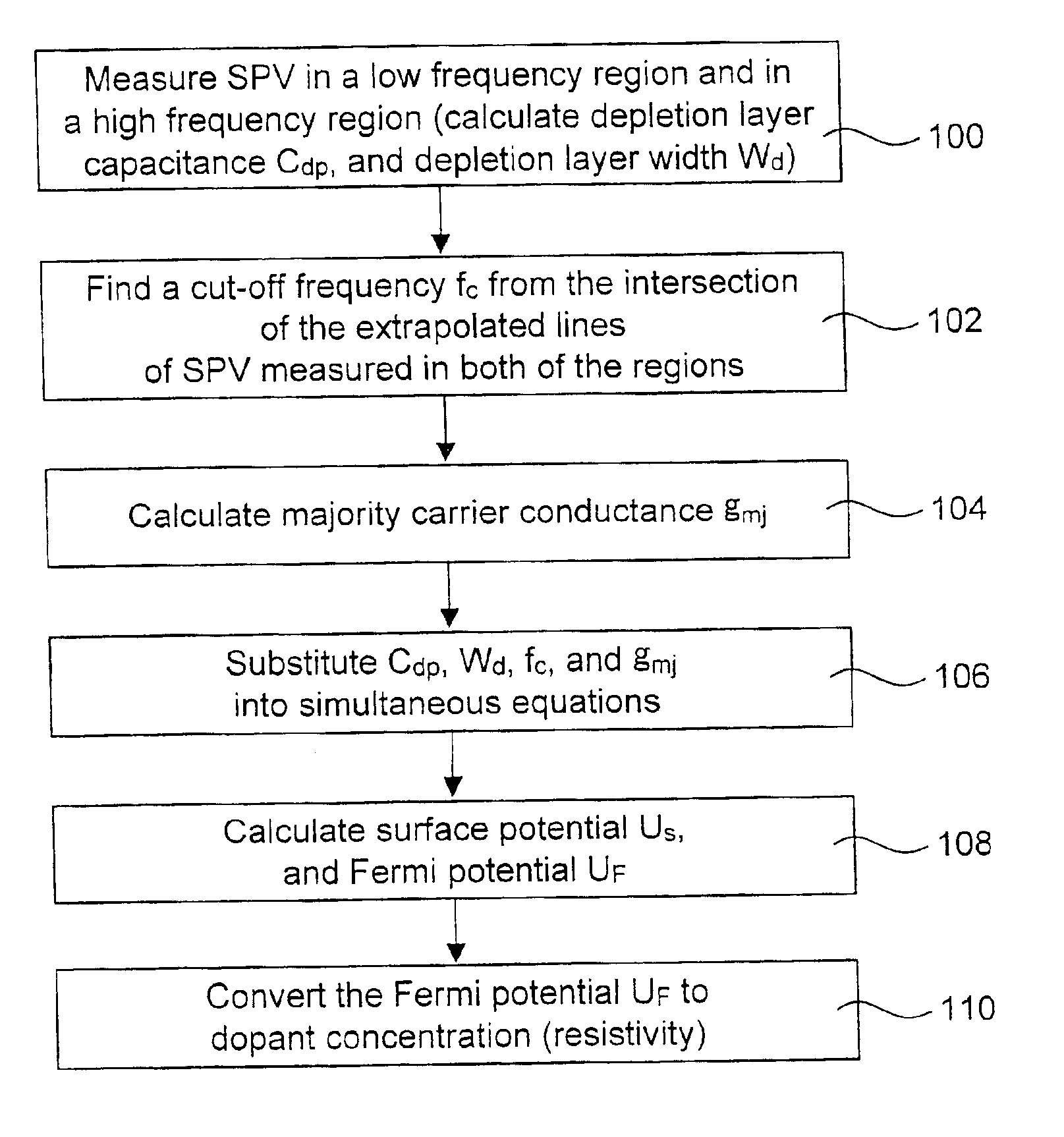
[0058]Resistivity (dopant concentration) of an epitaxial wafer having an epitaxial layer (thickness: 3 μm) with a p-type of conductivity and unknown resistivity was measured by the measuring method of the present invention in the following manner.

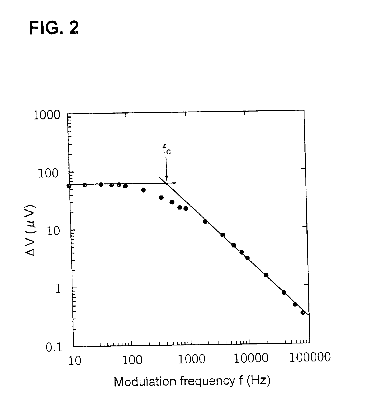
[0059]First, the epitaxial wafer just after epitaxial growth was placed on an SPV measuring device and subjected to ROST and then SPV was measured in a low frequency region and a high frequency region. The frequencies of an incident light in the low frequency region and the high frequency region were 10 Hz and 50 kHz, respectively.

[0060]By drawing lines extrapolated from the SPV values measured in the respective regions, as shown in FIG. 2, the cut-off frequency fc of 3.31 kHz was obtained. Moreover, from the measured values in the high frequency region, the depletion layer capacitance Cdp of 6.19 nF was obtained and hence the depletion layer width Wd of 1.67 μm was calculated from the equation (5). Then, by substituting fc=3.31 kHz and Cdp...


PUM


Abstract

The present invention is to provide a method for measuring resistivity of a semiconductor wafer by the use of an AC-SPV method even though the wafer is left in a depletion state or a weak inversion state. The present invention is the method for measuring resistivity of a semiconductor wafer by the use of a surface photo voltage method, and comprises the steps of: (a) measuring a surface photo voltage value in both regions of a low frequency region in which a constant surface photo voltage value is obtained irrespective of a frequency of incident light on a semiconductor wafer to be measured and in a high frequency region in which the surface photo voltage value inversely proportional to the frequency of the incident light is obtained and calculating a cut-off frequency fc from the obtained measured value; (b) calculating a depletion layer width Wd from capacitance Cdp calculated from the surface photo voltage value in the high frequency region; (c) calculating majority carrier conductance gmj from the cut-off frequency fc and the capacitance Cdp; and (d) calculating surface potential Us and Fermi potential UF from the cut-off frequency fc, the capacitance Cdp, the depletion layer width Wd, and the majority carrier conductance gmj.

Description

TECHNICAL FIELD[0001]The present invention relates to a method for measuring resistivity of a semiconductor wafer (hereinafter, in some cases, referred to as a wafer) by the use of surface photo voltage method.BACKGROUND ART[0002]A method for utilizing surface photo voltage (hereinafter, referred to as SPV) is proposed as a method for measuring resistivity of a semiconductor wafer in a noncontact manner by Emil Kamieniecki et al, for example, in J. Appl. Phys. Vol. 54 (11), November 1983, p. 6481. The SPV means a change in surface potential produced when a semiconductor is irradiated with light. The SPV excited by the use of a photon beam intermittently chopped at an appropriate frequency as incident light is called alternating current SPV (AC-SPV). In the present specification, the SPV means the AC-SPV, unless otherwise specified.[0003]First, one example of a device for measuring the SPV will be described with reference to FIG. 4. In FIG. 4, reference numeral 10 denotes a device fo...

Claims


Application Information

Patent Timeline
Patent Type & Authority Patents(United States)
IPC IPC(8): G01R31/26G01R27/02G01R31/302H01L21/66
CPCG01R31/2648
Inventor EBARA, KOJI
Owner SHIN-ETSU HANDOTAI CO LTD
Why Eureka
Try Eureka