Semiconductor memory device with memory cell array divided into blocks

a memory cell array and semiconductor technology, applied in the field of semiconductor memory devices, can solve the problems of slow data-read speed of memory cells, and achieve the effects of reducing the number of buffers, reducing the length of data signal lines and redundancy signal lines, and reducing the load capacitance of signal lines

Inactive Publication Date: 2005-07-05
FUJITSU SEMICON LTD
View PDF5 Cites 3 Cited by
  • Summary
  • Abstract
  • Description
  • Claims
  • Application Information

AI Technical Summary

Benefits of technology

[0027]In the semiconductor memory device described above, the first multiplexer performs block selection, and, then, the second multiplexer carries out redundancy processing. This provision allows a buffer for driving the redundancy signal to be provided between the first multiplexer and the second multiplexer for the purpose of driving the redundancy signal having undergone the block selection. The number of buffers can thus be reduced compared with the related-art construction in which such buffers are provided for all the redundancy signals that are not yet subjected to block selection.
[0028]The first multiplexer may be provided as many as at least two, and each of such first multiplexers may be coupled to corresponding ones of the blocks. With this provision, the first multiplexers can be situated closer to the corresponding ones of the blocks than the second multiplexer is situated. This reduces the length of the data signal lines and the redundancy signal line, compared with conventional constructions. This reduces the load capacitance of the signal lines, thereby improving the data-read speed of memory cells.

Problems solved by technology

Further, the distance from each block (the memory cell arrays 11-0 through 11-3) to the multiplexer 13 is long, which gives rise to a problem in that the data signal lines 18-0 through 18-3 end up having the heavy capacitance load, resulting in slower data-read speed of memory cells.

Method used


Image

  • Semiconductor memory device with memory cell array divided into blocks
  • Semiconductor memory device with memory cell array divided into blocks
  • Semiconductor memory device with memory cell array divided into blocks

Examples


Embodiment Construction

[0037]In the following, embodiments of the present invention will be described with reference to the accompanying drawings.

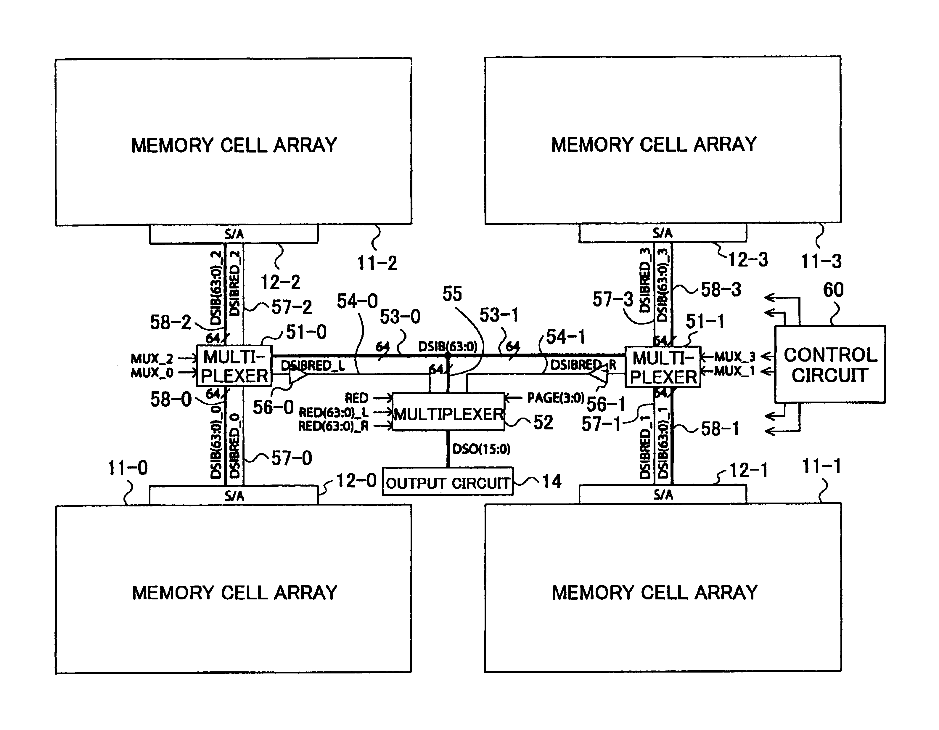
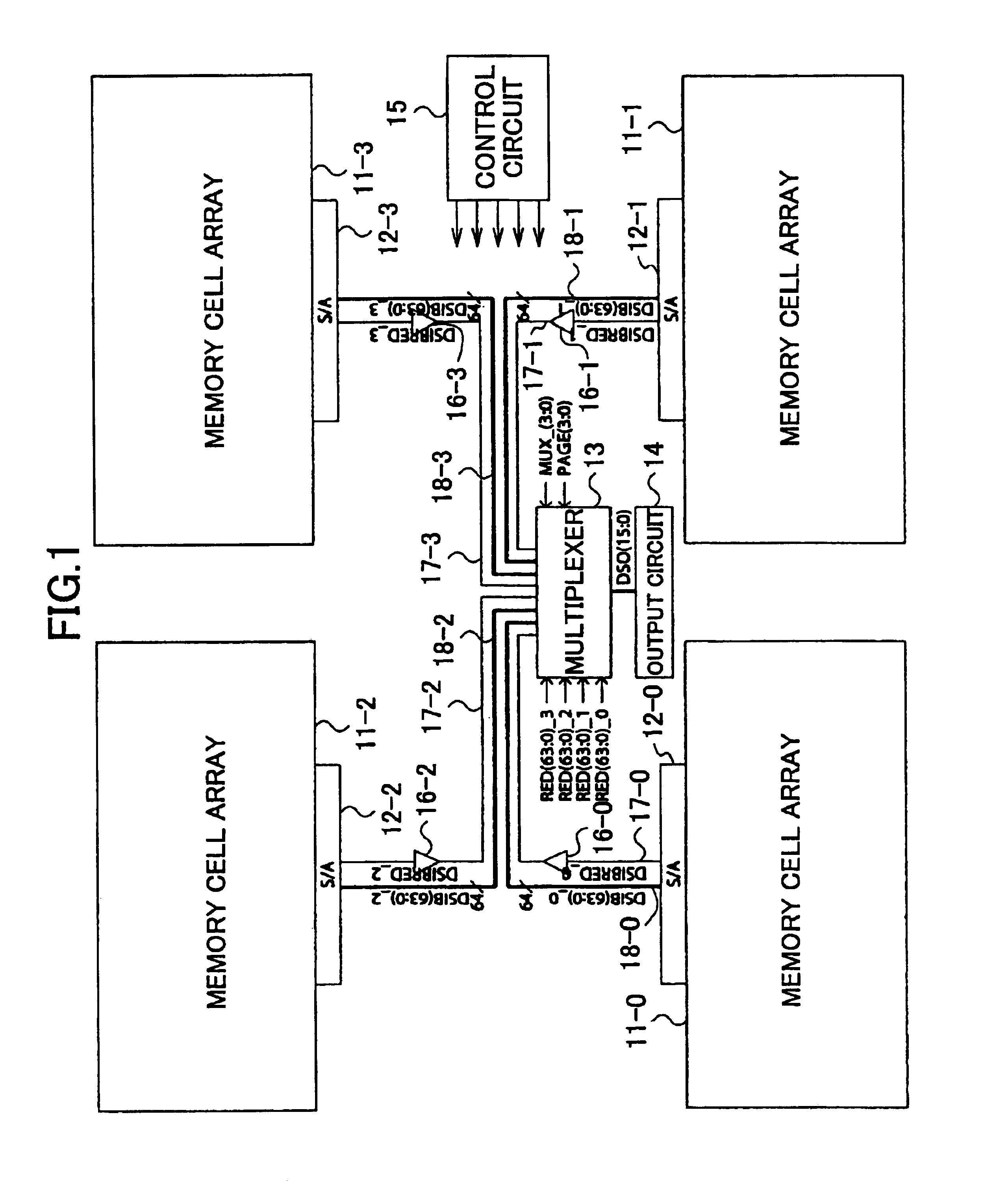
[0038]FIG. 4 is a block diagram showing an example of the construction of a semiconductor memory device according to the invention in which the memory cell block is divided into a plurality of blocks.

[0039]The semiconductor memory device of FIG. 4 includes memory cell arrays 11-0 through 11-3, sense amplifiers 12-0 through 12-3, an output circuit 14, multiplexers 51-0 and 51-1, a multiplexer 52, data signal lines 53-0 and 53-1, redundancy bit signal lines 54-0 and 54-1, data signal lines 55, buffers 56-0 and 56-1, redundancy bit signal lines 57-0 through 57-3, data signal lines 58-0 through 58-3, and a control circuit 60.

[0040]The memory cell arrays 11-0 through 11-3 include memory cells arranged in rows and columns, a plurality of word lines, a plurality of bit lines, an X decoder for selecting a word line, and a Y decoder for selecting a Y address. Data access...


PUM


Abstract

A semiconductor memory device includes a plurality of blocks, each of which includes a memory cell array, and outputs data signals and a redundancy signal. The semiconductor memory device further includes at least one first multiplexer which is coupled to the blocks, and selects one of the blocks, and a second multiplexer which performs redundancy processing based on the data signals and the redundancy signal which have undergone block selection by the first multiplexer.

Description

CROSS-REFERENCE TO RELATED APPLICATIONS[0001]The present application is based upon and claims the benefit of priority from the prior Japanese Patent Application No. 2002-268314 filed on Sep. 13, 2002, with the Japanese Patent Office, the entire contents of which are incorporated herein by reference.BACKGROUND OF THE INVENTION[0002]1. Field of the Invention[0003]The present invention generally relates to semiconductor memory devices, and particularly relates to a semiconductor memory device in which a memory cell array is divided into a plurality of blocks.[0004]2. Description of the Related Art[0005]In semiconductor memory devices such as DRAMs (Dynamic Random Access Memories) and flash memories, a memory cell array is divided into a plurality of blocks, with peripheral circuits of the memory core such as an X decoder, a Y decoder, and sense amplifiers being provided separately for each block. Such division into blocks brings about advantages such as high-speed data access by reduci...

Claims


Application Information

Patent Timeline
Patent Type & Authority Patents(United States)
IPC IPC(8): G11C11/22G11C11/401G11C7/00G11C7/10G11C11/4063G11C29/00G11C29/04G11C8/12G11C11/4096
CPCG11C7/1012G11C7/1051G11C29/846G11C11/4096G11C8/12G11C7/10
Inventor CHEUNG, ANDYOKA, YASUSHI
Owner FUJITSU SEMICON LTD
Why Eureka
Try Eureka