Method for producing a nitride semiconductor element

a technology of nitride and semiconductor elements, which is applied in the direction of semiconductor lasers, semiconductor laser structural details, lasers, etc., can solve the problems of limited structure of nitride semiconductor elements, difficulty in producing a bulk of single crystals, sapphire is a low thermal conductivity insulating material, etc., to reduce the area cutting off light, reduce the size of the n-type terminal, and improve the outgoing efficiency of ligh

Inactive Publication Date: 2005-07-12
NICHIA CORP
View PDF8 Cites 70 Cited by
  • Summary
  • Abstract
  • Description
  • Claims
  • Application Information

AI Technical Summary

Benefits of technology

[0011]The nitride semiconductor element of the invention includes, at least a conductive layer, a first terminal, a nitride semiconductor with a light-emitting layer, and a second terminal, from a supporting substrate successively, wherein, the first terminal and a first insulating protect layer are interposed between the conductive layer and a first conductive type nitride semiconductor layer. The nitride semiconductor may include the first conductive type nitride semiconductor layer, the light-emitting layer, and a second conductive type nitride semiconductor layer, which has an asperity portion as a top layer thereof. When the supporting substrate is conductive material, it can provide the nitride semiconductor element with an opposed terminal structure. In addition, when the first terminal is a p-type terminal, it can improve the outgoing efficiency of the light. That is, the second conductive type nitride semiconductor element formed in the second terminal (n-type terminal) side, which is topside of the nitride semiconductor layer, is an n-type nitride semiconductor layer. In other word, the n-type nitride semiconductor layer side is the outgoing surface of the light. An n-type layer in the nitride semiconductor (especially GaN system semiconductor) is of low resistance, so that the size of the n-type terminal, the second terminal, can be downsized. Because downsizing the size of the n-type terminal reduce the area cutting off the light, it can improve the outgoing efficiency of the light. Additionally, the conventional nitride semiconductor element has a structure having both terminals in the same plane side, so that it is required to provide a p-pad terminal for the p-type terminal. When conductive material is employed as the supporting substrate in the invention, die-bonding to a package such as a lead frame with a conductive material can achieve continuity. Therefore the p-pad terminal can be eliminated, it can increase the area of light-emission. In addition, providing the first insulating protect layer can prevent short circuit, etc., so that it can improve yield and reliability. It can also simplify its producing process.
[0012]In the nitride semiconductor element of the invention, the first terminal and the first insulating protect layer are in contact with the first conductive type nitride semiconductor layer. The first terminal may be formed on the whole of the first conductive type nitride semiconductor layer, however, it should be appreciated that forming the first terminal partially and covering an opening portion with the first insulating protect layer can adjust the contact area between the first terminal and the first conductive type nitride semiconductor layer. In addition, forming the first terminal in a pattern such as a rectangular shape, lines, a square shape, a grid pattern, dots, a rhombus, a parallelogram, a mesh shape, a striped shape, a ramose shape branching from one into a plurality of branches, etc. can improve the outgoing efficiency of the light. When the first conductive type nitride semiconductor layer can have ohmic contact with the first terminal, either p-type terminal or n-type terminal can be employed as the first conductive type nitride semiconductor layer. The first conductive type nitride semiconductor layer is not restricted either in a single-layer or a multi-layer.
[0013]The first terminal includes at least one element selected from the group of Ag, Rh, Ni, Au, Pd, Ir, Ti, Pt, W, and Al. Concretely, reflectivity of Ag, Al, Rh, Pd, and Au are 89%, 84%, 55%, 50%, and 24%, respectively. Thus, according to the reflectivity Ag is the most preferable material, however, it is preferable to employ Rh in view of ohmic contact when the first conductive type nitride semiconductor layer is p-type. Using the material can achieve low resistance, and can improve the outgoing efficiency of the light. The conductive layer is formed of eutectic, which includes at least one element selected from the group of Au, Sn, and In. Employing the eutectic material as the conductive layer can form the layers even at low temperature. The eutectic junction can attach at low temperature, so that it can achieve an effect for reducing warpage. Additionally, employing the structure of (intimate-contact layer) / (barrier layer) / (eutectic layer) formed of Au, Sn, Pd, In, Ti, Ni, W, Mo, Au—Sn, Sn—Pd, In—Pd, Ti—Pt—Au, and Ti—Pt—Sn, etc. from the first terminal side can prevent deterioration cause of the diffusion from the first terminal (p-type terminal, for example).

Problems solved by technology

A nitride semiconductor is one of desirable candidate direct-band-gap semiconductor materials, however, it is difficult to produce a bulk of its single crystal.
However, sapphire is a low thermal conductivity insulating material.
Thus, the structure of nitride semiconductor element is limited.
Therefore, when an insulating material such as sapphire, etc. is employed as a substrate, it reduce the effective area of light-emission compared with a conductive substrate having the same area of substrate.
In addition, wires are required for both of pn terminals in a wire-bonding process for the terminals, so that it increases chip size.
Therefore it reduces yield of chips.

Method used


Image

  • Method for producing a nitride semiconductor element
  • Method for producing a nitride semiconductor element
  • Method for producing a nitride semiconductor element

Examples


embodiment 1

[0104]The following description will describe a process of producing an embodiment of the nitride semiconductor element according to the invention with reference to the drawings.

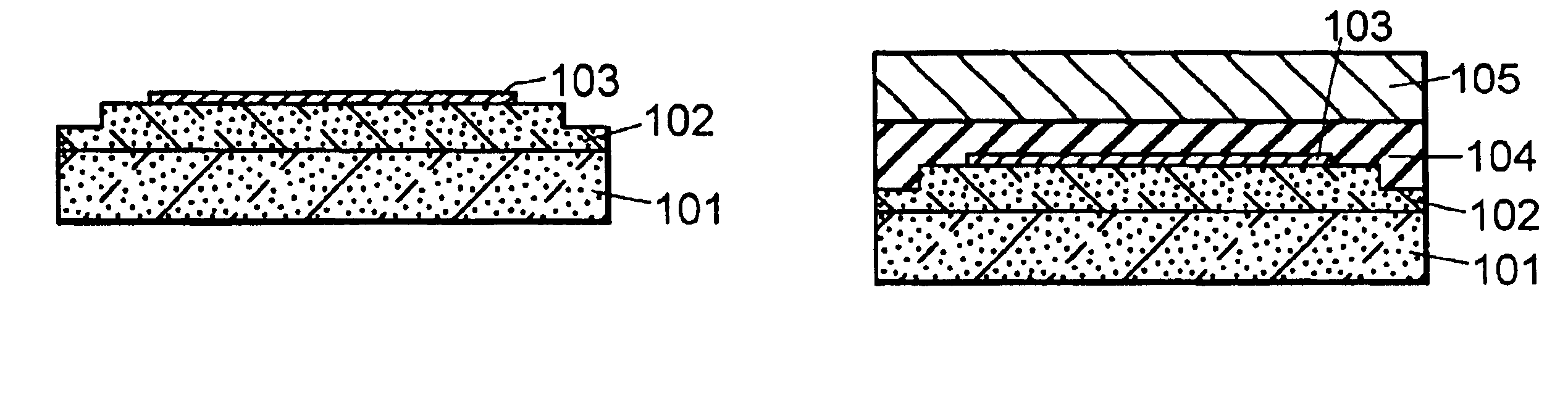
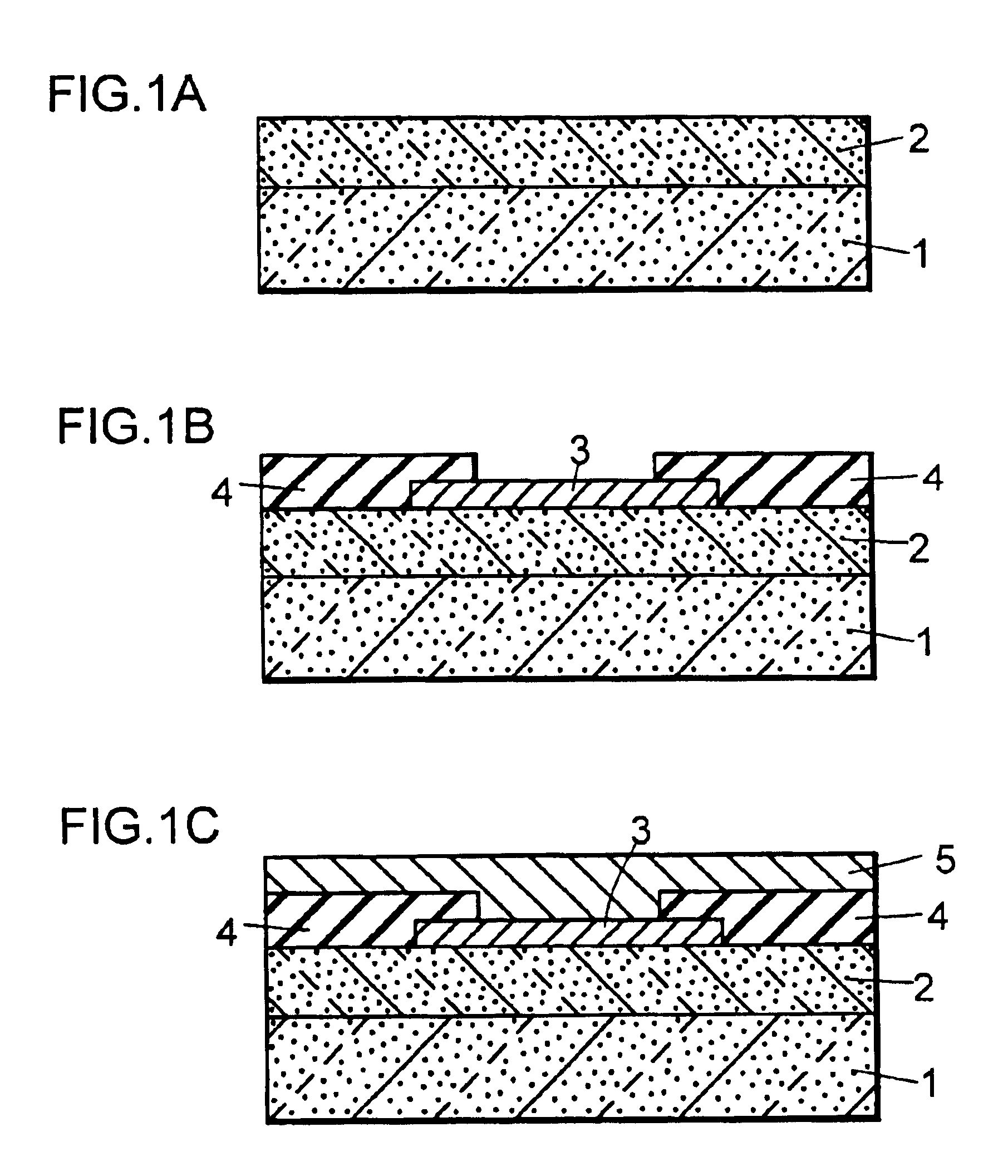
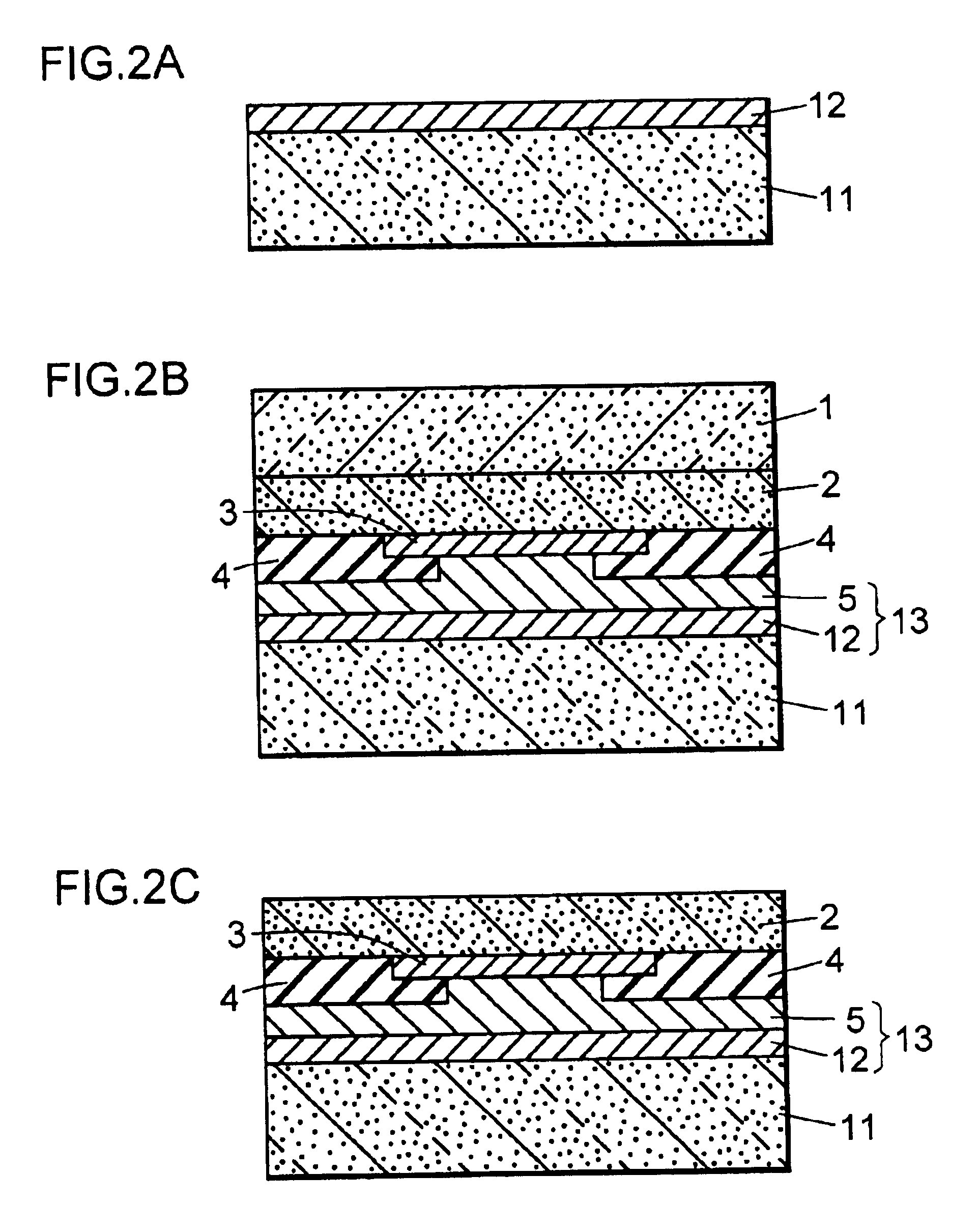
[0105]The nitride semiconductor 2 including at least a second conductive type nitride semiconductor layer, a light-emitting layer, a first conductive type nitride semiconductor layer is grown on a different material substrate 1 such as sapphire (FIG. 1A). Subsequently, a first terminal 3 (p-type terminal, for example) is formed on the nitride semiconductor layers. Next, a first insulating protect layer 4 is formed on an opening portion, or an exposed portion of the nitride semiconductor (FIG. 1B). Further, a conductive layer 5 for alloying at attachment is formed (FIG. 1C). It is preferable that the conductive layer has a three-layer structure composed of an intimate-contact, a barrier layer, and a eutectic layer. On the other hand, a supporting substrate 11 is prepared. It is preferable that a conductive la...

embodiment 2

[0137]A nitride semiconductor 2 is formed on or above a different material substrate 1, as a second conductive type nitride semiconductor layer, a light-emitting layer, a first conductive type nitride semiconductor layer successively. First, the surface is etched partly by RIE, etc. Subsequently, it is annealed under atmosphere with oxygen. A first terminal with high reflectivity and capable of ohmic contact with the first conductive type nitride semiconductor layer is pattern-formed on the surface, which is not etched. Next, a first insulating protect layer is formed on the part, on where the first terminal is not formed. SiO2, etc. can be employed as material of the protect layer, and a multi-layer structure of them can also be employed. A metal layer with high reflectivity such as Al can be formed further on there. Then, a conductive layer composed of an intimate layer, a barrier layer, and an eutectic layer, can be formed on the whole of wafer or the part, where is not etched. T...

embodiment 3

[0140]In the nitride semiconductor element of this embodiment, the attachment process is performed twice (FIG. 13). A method for producing a nitride semiconductor element having at least a first terminal, a nitride semiconductor with a light-emitting layer, and a second terminal on or above a supporting substrate successively, includes: a first step for growing the nitride semiconductor with the light-emitting layer on or above a first substrate; subsequently, a second step for eliminating the first substrate and forming an exposed surface of the nitride semiconductor; subsequently, a third step forming a asperity on the exposed surface; subsequently, a forth step for attaching the supporting substrate to the exposed surface of the nitride semiconductor layer with interposing; and subsequently a fifth step for eliminating the second substrate.

[0141]In the first step, the second substrate is attached to the growth surface of the nitride semiconductor layer with interposing the second...


PUM

PropertyMeasurementUnit
refractive indexaaaaaaaaaa
wavelength of lightaaaaaaaaaa
wavelengthaaaaaaaaaa

Abstract

A method of producing an efficient nitride semiconductor element having an opposed terminal structure. The method includes a growing step for growing the nitride semiconductor further having an undoped GaN layer on a different materials substrate; subsequently, an attaching step for attaching the supporting substrate to the first conductive type nitride semiconductor layer side of the nitride semiconductor and interposing a first terminal between them; and subsequently, an exposing step for exposing the second conductive type nitride semiconductor layer by eliminating the different material substrate and the undoped GaN.

Description

[0001]This is a Divisional Application of U.S. application Ser. No. 10 / 351,497, filed Jan. 27, 2003 now U.S. Pat. No. 6,744,071.[0002]This application is based on Application No. 2002-019192 filed in Japan on Jan. 28, 2002, No. 2002-195179 filed in Japan on Jul. 3, 2002, No. 2002-356463 filed in Japan on Dec. 9, 2002, No. 2002-175686 filed in Japan on Jun. 17, 2002, No. 2002-233866 filed in Japan on Aug. 9, 2002, the contents of which are incorporated hereinto by references.FILED OF THE INVENTION[0003]This invention relates to a nitride semiconductor element with a supporting substrate used for a light-emitting device such as a light emitting diode (LED), a laser diode (LD), etc., a photoreceptor such as a solar cell, a photo sensor, etc., an electronic device such as a transistor, a power device, etc., and a method for producing thereof. An attaching structure is employed as one of the methods for producing.BACKGROUND OF THE INVENTION[0004]A nitride semiconductor is one of desirabl...

Claims


Application Information

Patent Timeline
Patent Type & Authority Patents(United States)
IPC IPC(8): H01L33/00H01L33/62H01L27/15H01L29/16H01L29/26H01L33/06H01L33/10H01L33/20H01L33/22H01L33/32H01L33/38H01L33/40H01L33/44H01S5/00H01S5/02H01S5/022H01S5/024H01S5/042H01S5/183H01S5/30H01S5/343
CPCB82Y20/00H01L33/0079H01L33/22H01L33/32H01L33/38H01L33/405H01L33/44H01L33/10H01L33/382H01L33/387H01L33/46H01L2933/0016H01S2304/12H01L2224/48091H01L2924/00014H01L2224/49113H01L2224/45144H01L2924/00H01L33/0093
Inventor SANO, MASAHIKONONAKA, MITSUHIROKAMADA, KAZUMIYAMAMOTO, MASASHI
Owner NICHIA CORP
Why Eureka
Try Eureka