Reliable low-k interconnect structure with hybrid dielectric

a hybrid dielectric and low-k technology, applied in semiconductor devices, semiconductor/solid-state device details, electrical apparatus, etc., can solve the problems of limiting the overall circuit speed, and affecting the overall circuit performance of the circuit, so as to achieve the effect of limiting the overall circuit performance, limiting the interconnect delay, and limiting the overall circuit speed

Inactive Publication Date: 2005-07-12
GLOBALFOUNDRIES US INC
View PDF32 Cites 51 Cited by
  • Summary
  • Abstract
  • Description
  • Claims
  • Application Information

AI Technical Summary

Problems solved by technology

High speed logic chips require faster interconnects, as the interconnect delay is now limiting the overall circuit speed.
With scaling to smaller dimensions, the interconnect delay becomes a more significant factor limiting overall circuit performance.
However, copper interconnect structures using such low-k materials as the ILD can suffer from reliability problems, including mechanical failure caused by thermal expansion of the low-k dielectric materials.
This difference has been shown to significantly contribute to such reliability problems.
Finally, the manufacture of this structure is made very difficult by using the same multi-layer ILD for the via level and the line level, with no intermediate cap layer or etch stop layer.

Method used


Image

  • Reliable low-k interconnect structure with hybrid dielectric
  • Reliable low-k interconnect structure with hybrid dielectric
  • Reliable low-k interconnect structure with hybrid dielectric

Examples


Embodiment Construction

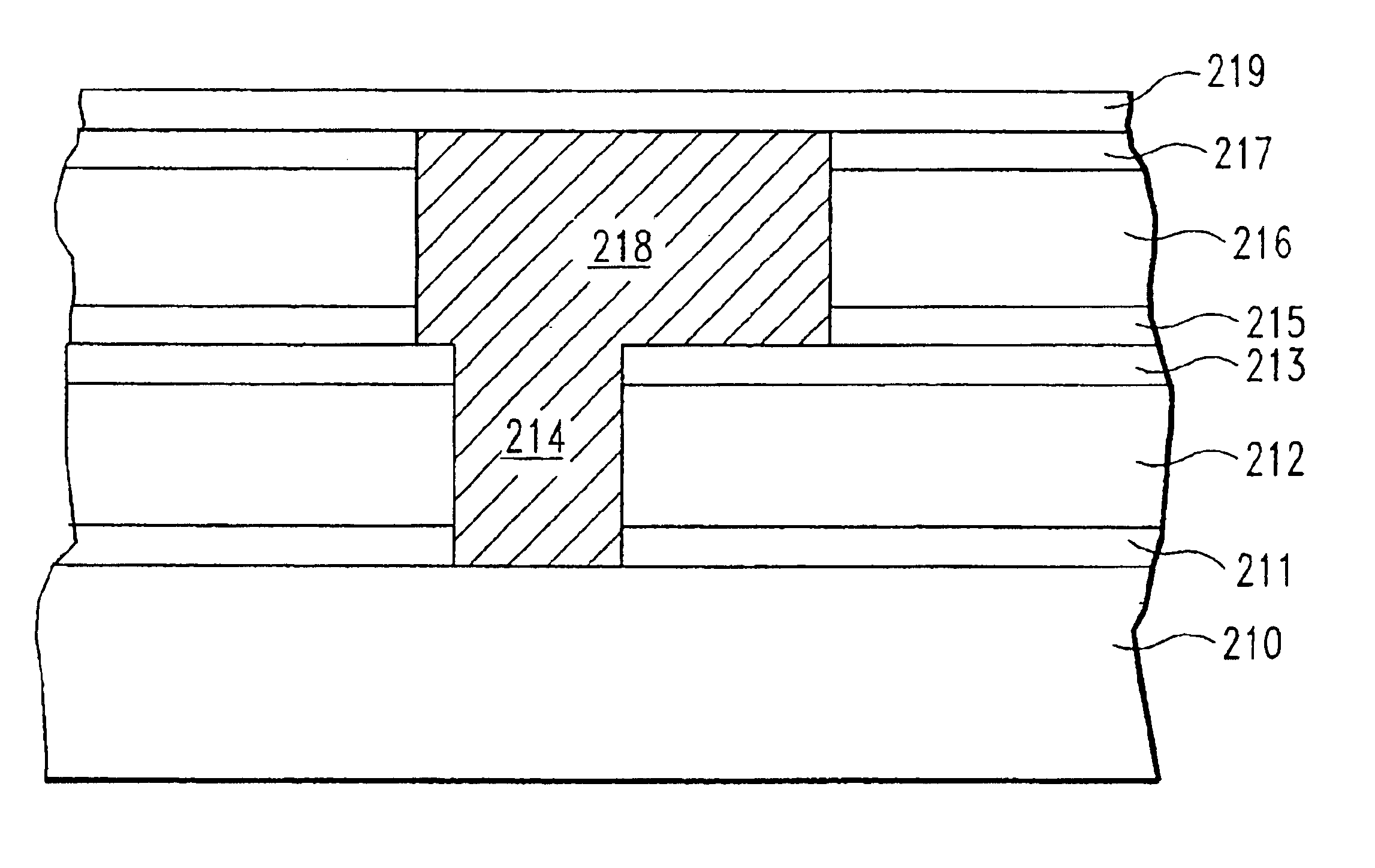
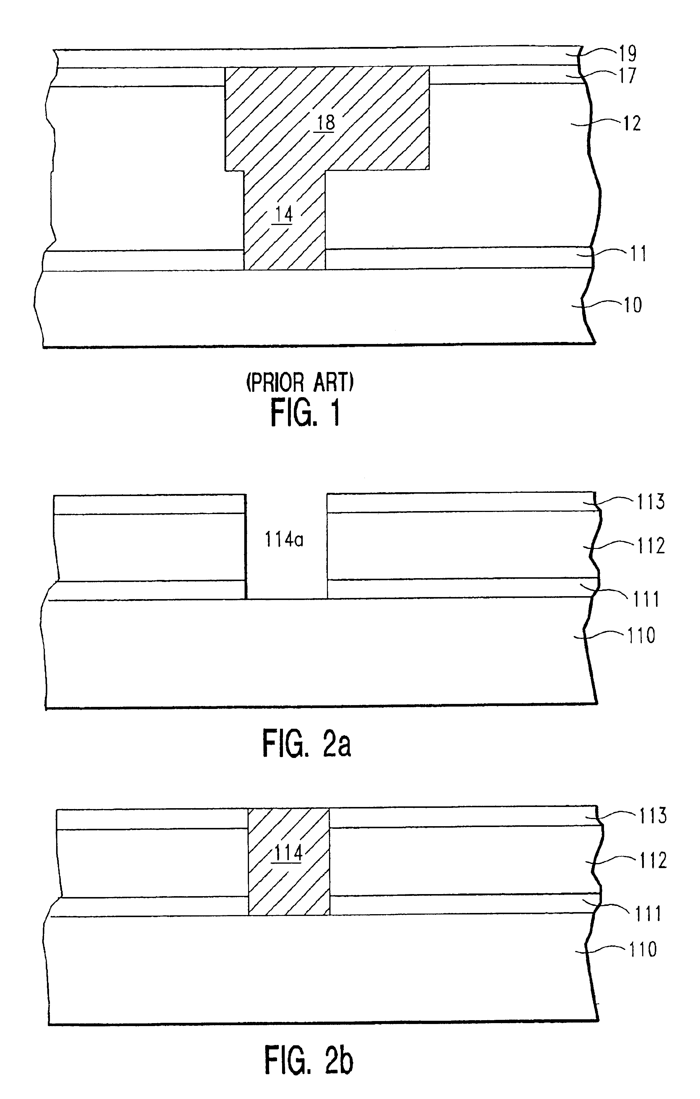
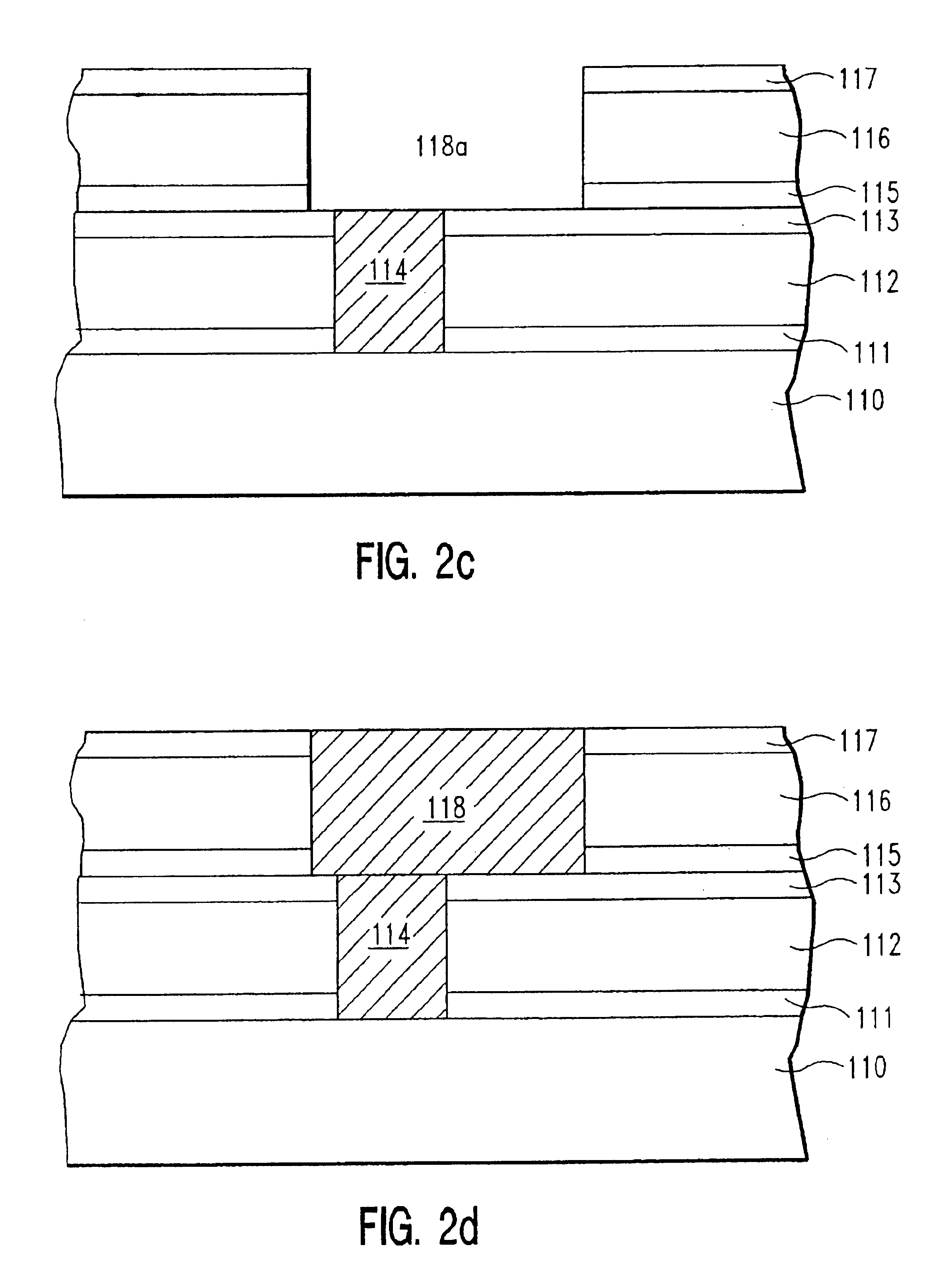
[0019]The invention will now be described by reference to the accompanying figures. In the figures, various aspects of the structures have been shown and schematically represented in a simplified manner to more clearly describe and illustrate the invention. For example, the figures are not intended to be to scale. In addition, the vertical cross-sections of the various aspects of the structures are illustrated as being rectangular in shape. Those skilled in the art will appreciate, however, that with practical structures these aspects will most likely incorporate more tapered features. Moreover, the invention is not limited to constructions of any particular shape.

[0020]Although certain aspects of the invention will be described with respect to a structure comprising copper, the invention is not so limited. Although copper is the preferred conductive material, the structure of the present invention may comprise any suitable conductive material, such as aluminum.

[0021]Referring to FI...


PUM


Abstract

An advanced back-end-of-line (BEOL) interconnect structure having a hybrid dielectric is disclosed. The inter-layer dielectric (ILD) for the via level is preferably different from the ILD for the line level. In a preferred embodiment, the via-level ILD is formed of a low-k SiCOH material, and the line-level ILD is formed of a low-k polymeric thermoset material.

Description

FIELD OF THE INVENTION[0001]This invention relates generally to the manufacture of high speed semiconductor microprocessors, application specific integrated circuits (ASICs), and other high speed integrated circuit devices. More particularly, this invention relates to advanced back-end-of-line (BEOL) metallization structures for semiconductor devices using low-k dielectric materials. The invention is specifically directed to an advanced BEOL interconnect structure having a hybrid dielectric with a low dielectric constant.BACKGROUND OF THE INVENTION[0002]Metal interconnections in very large scale integrated (VLSI) or ultra-large scale integrated (ULSI) circuits typically consist of interconnect structures containing patterned layers of metal wiring. Typical integrated circuit (IC) devices contain from three to fifteen layers of metal wiring. As feature size decreases and device area density increases, the number of interconnect layers is expected to increase.[0003]The materials and l...

Claims


Application Information

Patent Timeline
Patent Type & Authority Patents(United States)
IPC IPC(8): H01L23/52H01L23/532H01L21/768H01L21/70
CPCH01L21/76801H01L21/76807H01L21/76832H01L21/76835H01L23/53295H01L2924/0002H01L2924/00H01L21/768
Inventor FITZSIMMONS, JOHN A.GRECO, STEPHEN E.LEE, JIAGATES, STEPHEN M.SPOONER, TERRYANGYAL, MATTHEW S.HICHRI, HABIBSTANDAERT, THEORDORUS E.BIERY, GLENN A.
Owner GLOBALFOUNDRIES US INC
Why Eureka
Try Eureka