Digital adjustment of gain and offset for digital to analog converters

a digital to analog converter and gain adjustment technology, applied in the field of integrated circuits, can solve the problems of increasing the cost and power consumption of the device, reducing the flexibility of the device, and requiring a fairly large range of resistances

Inactive Publication Date: 2005-07-12
SEMTECH CORP
View PDF8 Cites 22 Cited by
  • Summary
  • Abstract
  • Description
  • Claims
  • Application Information

AI Technical Summary

Benefits of technology

[0006]The present invention is an improved

Problems solved by technology

First, it decreases the flexibility of the device since the integrated circuit manufacturer fixes the number of current and voltage outputs.
Alternatively, if user configuration of either current or voltage mode is desired, it increases the cost and power consumption of the device since two DACs would then be needed for a single output.
Also, since DACs may have a fairly large range of gains and offsets, a fairly larg

Method used


Image

  • Digital adjustment of gain and offset for digital to analog converters
  • Digital adjustment of gain and offset for digital to analog converters
  • Digital adjustment of gain and offset for digital to analog converters

Examples


Embodiment Construction

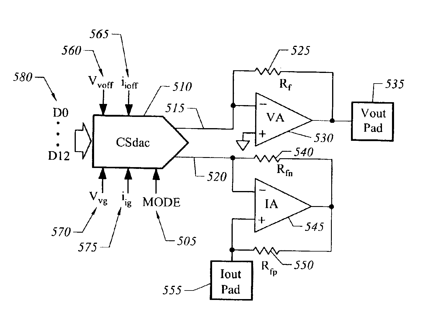
[0021]The present invention is directed to improved analog to digital conversion circuitry incorporating features that increase the flexibility and lower the cost. In particular, the ability to digitally adjust gain and offset is provided, and circuitry to allow a single converter to provide either a voltage output or a current output is provided.

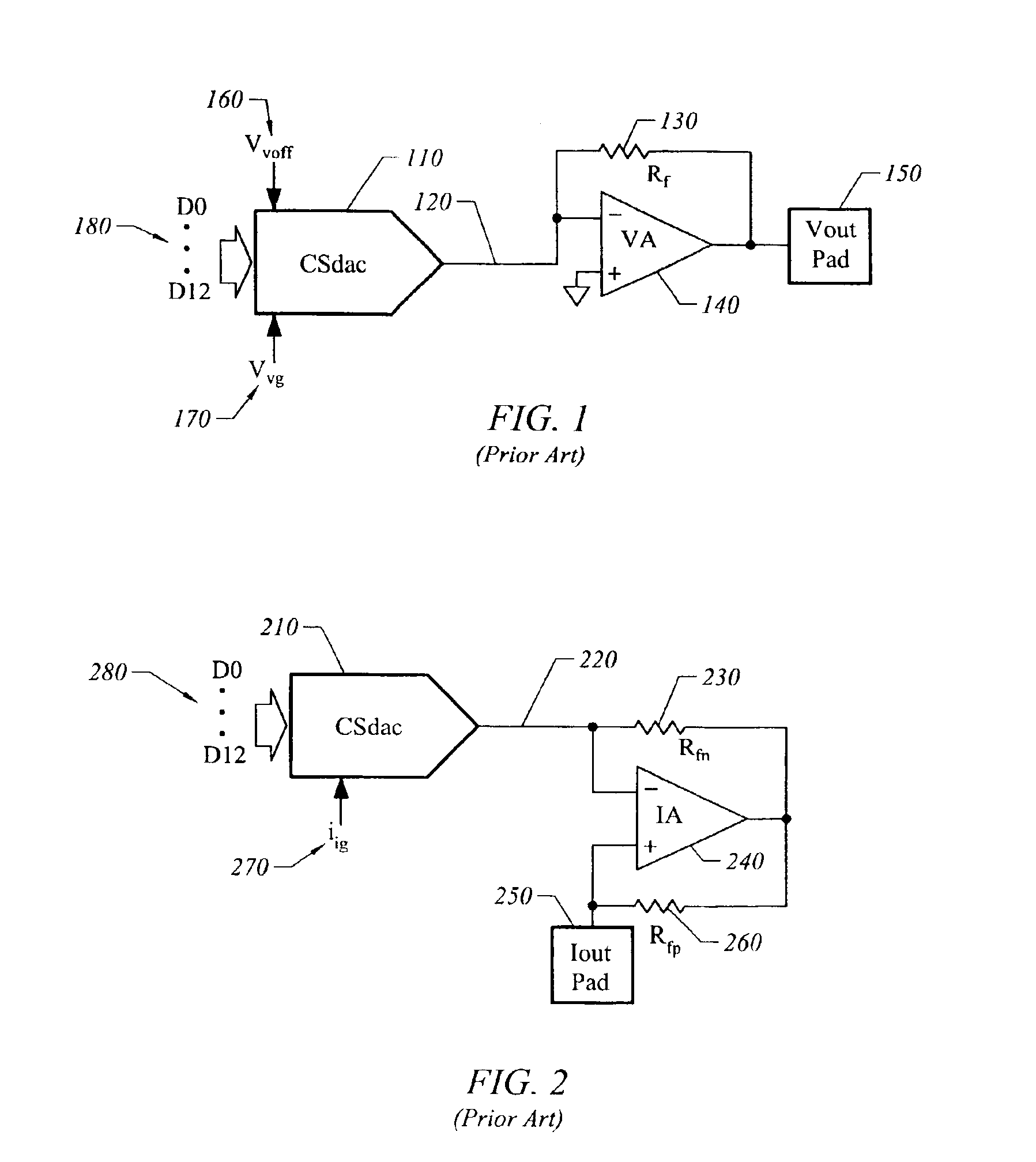
[0022]FIG. 1 illustrates a prior art voltage output digital to analog converter (DAC) circuitry. CSdac 110 is a current steering digital to analog converter (CSdac) that accepts digital input 180, voltage gain 170, voltage offset 160 and produces a current output on line 120, proportional to the binary value present on digital input 180. Current output 120 is coupled to the negative input of voltage amplifier 140 and to one side of feedback resistor 130. The positive input of voltage amplifier 140 is coupled to ground and the other side of feedback resistor 130 is coupled to the output of voltage amplifier 140. The output of voltage amplifi...


PUM


Abstract

Improved digital to analog converter (DAC) circuitry incorporating the ability to utilize a single DAC to generate either voltage or current outputs, and the ability to digitally adjust the gain and offset. Previous digital to analog circuitry has been limited to a single type of analog output per DAC and to the use of external precision resistors to set the gain and offset for a single DAC, or a group of DACs. By utilizing the same on-chip circuitry to supply both types of outputs, chip area, power consumption and cost is reduced while offering more flexibility to the customer. The ability to digitally adjust the gain and offset for a group of DACs eliminates the cost of external resistors, lowers the board area, and lowers the assembly cost for the end product. In addition, since gain and offset can be adjusted dynamically, maximum flexibility is provided to the customer. Digital adjustment of gain and offset can be used to calibrate for chip and system errors, and can allow more exact adjustment and external precision resistors.

Description

FIELD OF THE INVENTION[0001]The invention relates to the field of integrated circuits and more particularly to the field of digital to analog converter circuitry.BACKGROUND OF THE INVENTION[0002]Circuits that convert a digital value, such as a sequence of binary digits, to an analog value, such as voltage or current, are known generally as digital to analog converters, or DACs. The output of a DAC can be an analog voltage or an analog current. In a typical DAC, a binary value is written into a register and circuitry converts this value into a voltage or current, which is available as an output from the DAC. It is often desirable that the analog output vary linearly with the digital input, and in this case, the conversion of the binary value into the voltage or current is a function of the gain and offset of the DAC. The voltage output of a linear DAC can be expressed as:Vout=(Vgain·(DATA / MAX))+Voffsetand the current output of a linear DAC can be expressed as:Iout=(Igain·(DATA / MAX))+...

Claims


Application Information

Patent Timeline
IPC IPC(8): H03M1/10H03M1/66
CPCH03M1/1028H03M1/66
Inventor BLACKBURN, JEFFREY
Owner SEMTECH CORP
Why Eureka
Try Eureka