Illumination device with remote luminescent material

a luminescent material and illumination device technology, applied in semiconductor devices, point-like light sources, lighting and heating apparatuses, etc., can solve the problems of limited size of emitting sources, high brightness of sources, and inability to fit remote luminescent material modules in spot lamps, etc., to reduce system efficiency, reduce lifetime, and high brightness of sources

Active Publication Date: 2012-01-12
SIGNIFY HLDG BV
View PDF4 Cites 41 Cited by
  • Summary
  • Abstract
  • Description
  • Claims
  • Application Information

AI Technical Summary

Benefits of technology

[0008]For spot lamps, a high brightness of the source is required, i.e., for a requested luminous flux level the emitting source is limited in size to fit in a spot lamp. Typically the source size of a remote luminescent material module does not fit in a spot lamp. When reducing the remote luminescent material surface area to fit in the spot applications, the temperature of the remote luminescent material element may increase to unacceptable levels, leading to thermal quenching of the luminescent material...

Problems solved by technology

For spot lamps, a high brightness of the source is required, i.e., for a requested luminous flux level the emitting source is limited in size to fit in a spot lamp.
Typically the source size of a remote luminescent material module does not fit in a spot lamp.
When reducing the remote luminescent material surface area to fit in the spot applications, the temperature of the remote luminescent material element may increase to unacceptable levels, leading to thermal quenching of the luminescent material, which significantly reduces the system efficiency, and/or to material degradation (the luminescent material, or the matrix material comprising the luminescent material, or the substrate material that the luminescent material is applied onto) resulting in lumen depreciation, reduced lifetime and increased catastrophic system failures.
It appears that a relative high source brightness can be achieved with white LEDs where the wavelength converting material is applied on the LED chip, as this results in a small source size.
H...

Method used


Image

  • Illumination device with remote luminescent material
  • Illumination device with remote luminescent material
  • Illumination device with remote luminescent material

Examples


Embodiment Construction

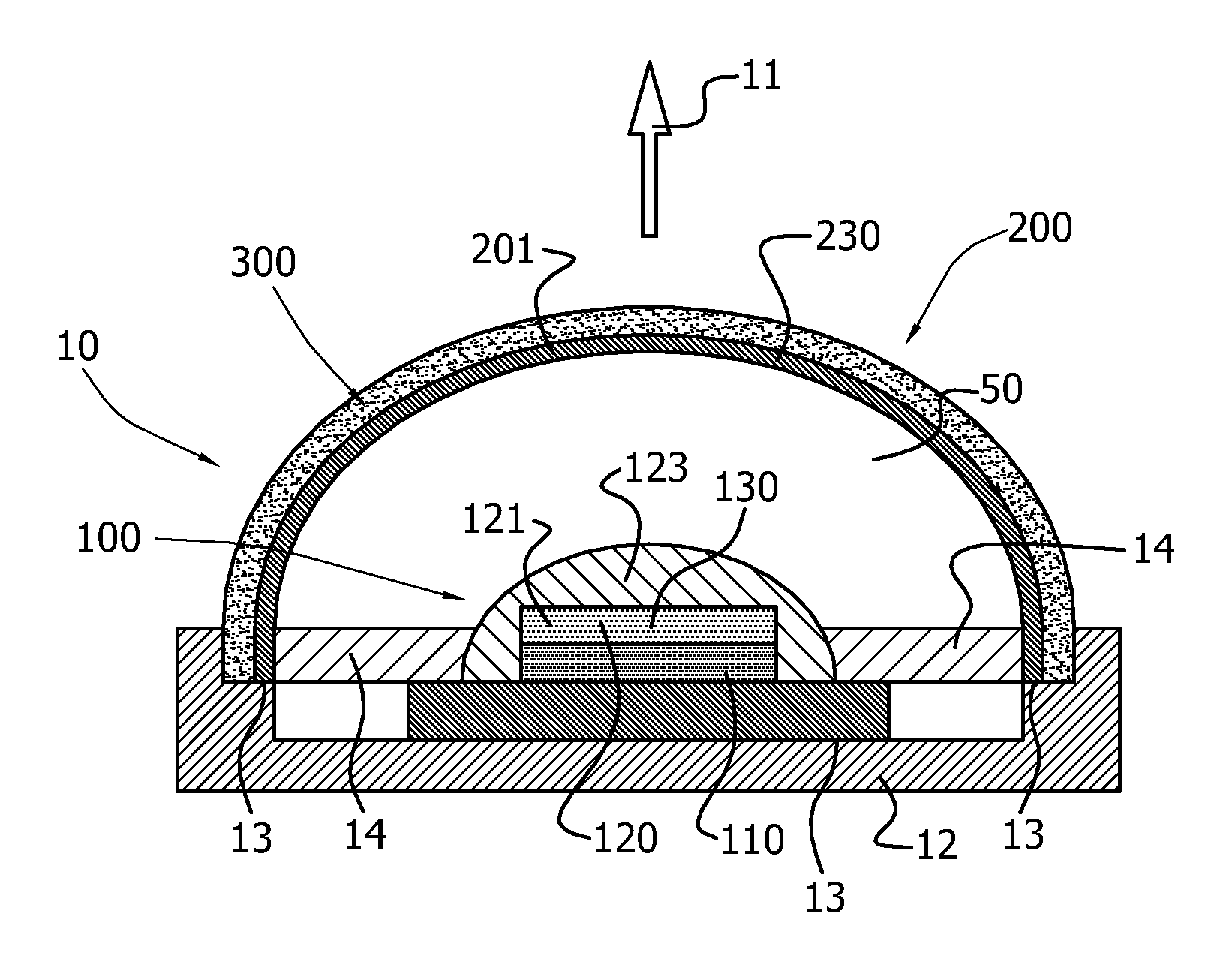
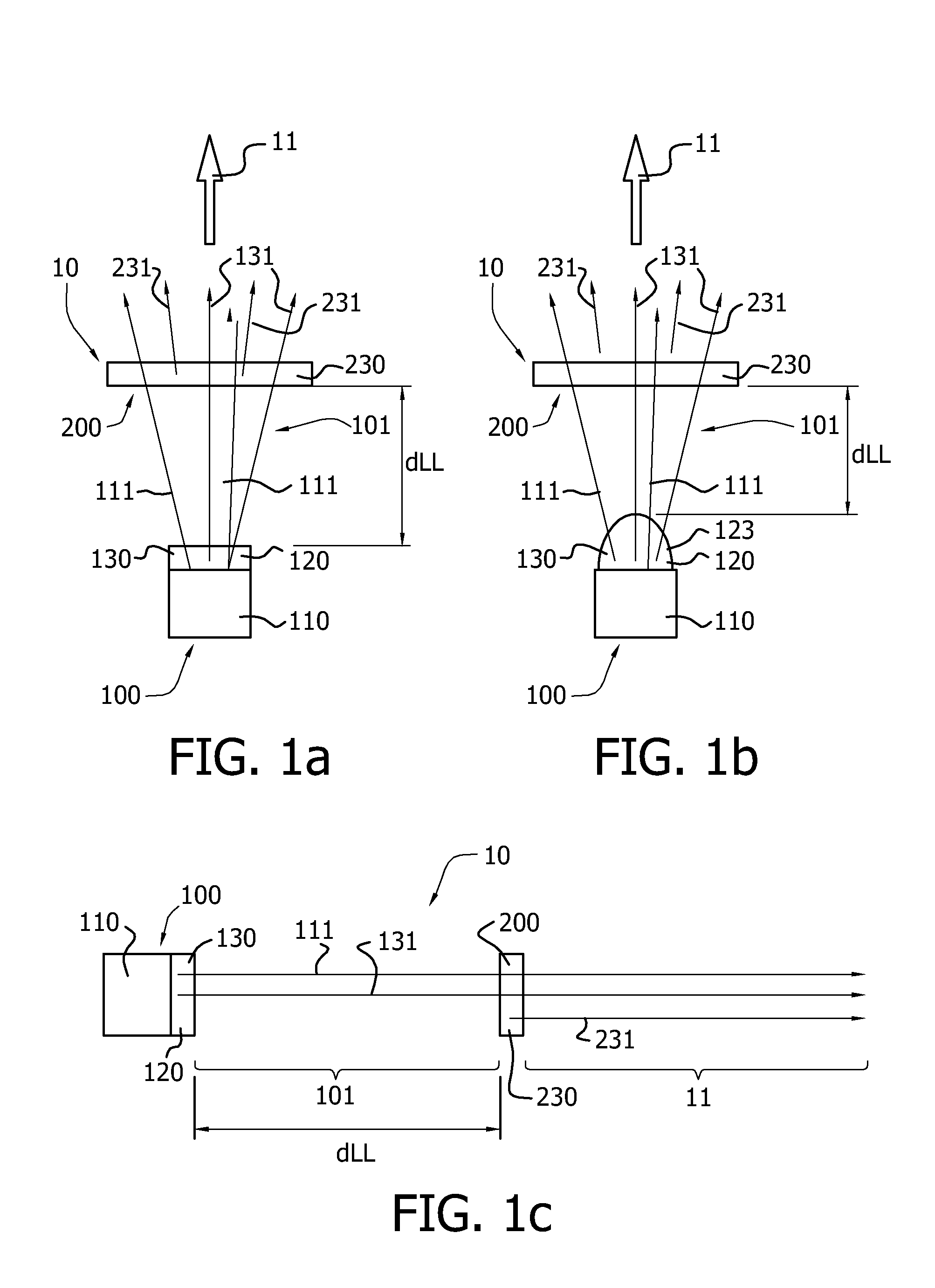
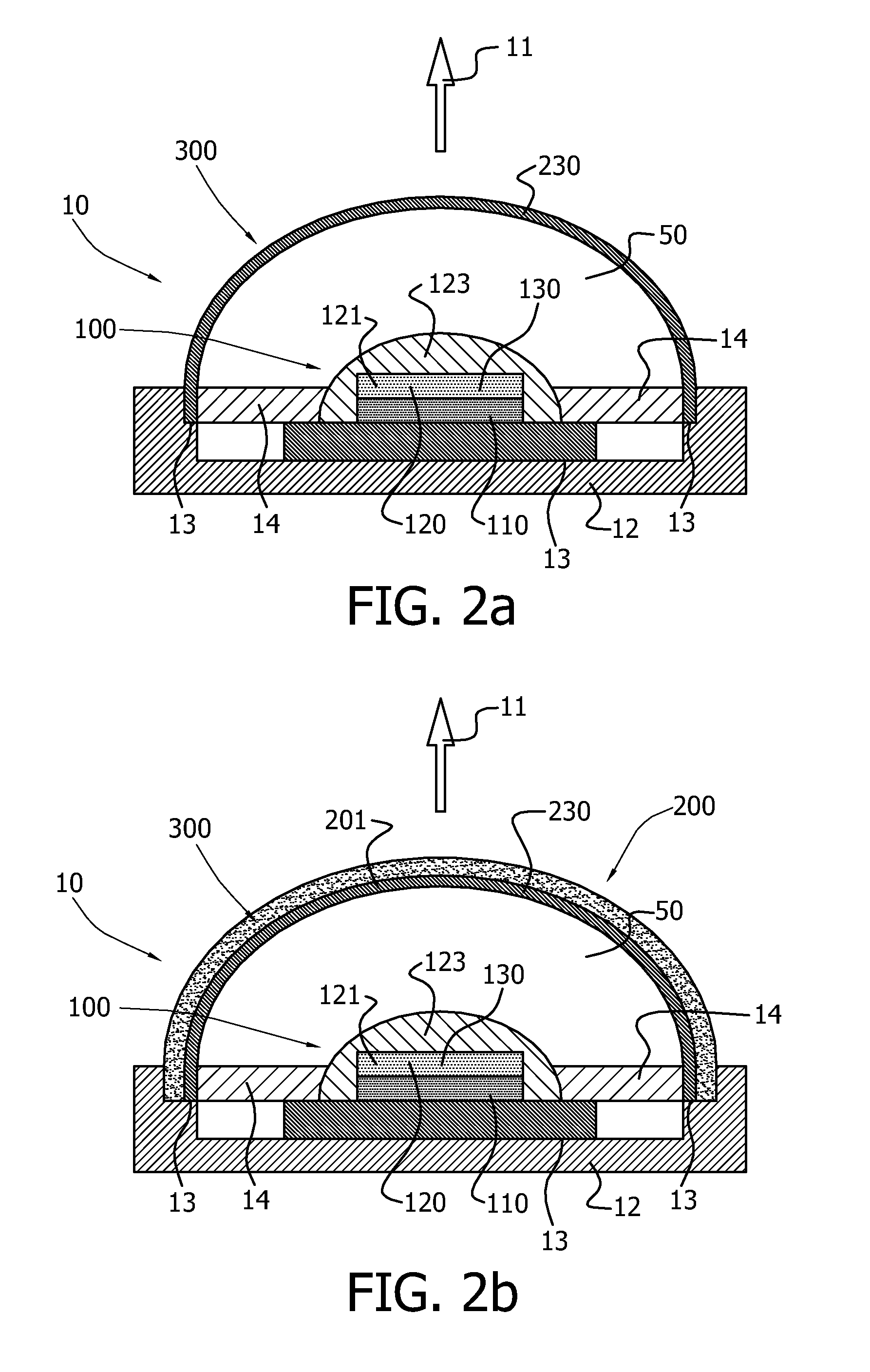
[0092]FIGS. 1a-1c schematically depict embodiments of an illumination device 10 according to the invention. The illumination device 10 comprises a light source 100 and a transmissive arrangement 200, remote from the light source 100. The light source 100 is arranged to generate light source light 101, and comprises a light emitting device (LED) 110, arranged to generate LED light 111 and a carrier 120 comprising a first luminescent material 130. The carrier 120 is in contact with the LED 110. The first luminescent material 130 is arranged to convert at least part of the LED light 111 into first luminescent material light 131.

[0093]The transmissive arrangement 200 of a second luminescent material 230 is arranged remote from the light source 100 and is arranged to convert at least part of the LED light 111 or at least part of the first luminescent material light 131, or at least part of the LED light 111 and at least part of the first luminescent material light 131 into second lumines...


PUM


Abstract

The invention provides an illumination device comprising a light source and a transmissive arrangement. The light source is arranged to generate light source light and comprises a light emitting device (LED), arranged to generate LED light and a carrier comprising a first luminescent material. The carrier is in contact with the LED and the first luminescent material is arranged to convert at least part of the LED light into first luminescent material light. The transmissive arrangement of a second luminescent material is arranged remote from the light source and is arranged to convert at least part of the LED light or at least part of the first luminescent material light and/or at least part of the LED light. The invention overcomes current limitations of remote luminescent material systems in spot lighting. In addition, an extremely simple way of realizing light sources with various correlated colour temperatures is allowed, based on just a single type of white (or whitish) light source in combination with various (red-orange) remote luminescent materials.

Description

FIELD OF THE INVENTION[0001]The invention relates to an illumination device comprising an LED based light source and a plurality of luminescent materials, with at least one luminescent material being arranged remote from the light source.BACKGROUND OF THE INVENTION[0002]Illumination devices comprising a transmissive arrangement with a luminescent material are known in the art. Transmissive ceramic layers or luminescent ceramics, and their method of preparation, are known in the art. It is for instance referred to US2005 / 0269582, US2006 / 0202105), to WO2006 / 097868, to WO2007 / 080555, to US2007 / 0126017 and to WO2006 / 114726.[0003]US2005 / 0269582 for instance, discloses a semiconductor light emitting device combined with a ceramic layer which is disposed in a path of light emitted by the light emitting layer. The ceramic layer is composed of or includes a wavelength converting material such as a luminescent material.[0004]Further, US2008029720 describes a lighting arrangement which compris...

Claims


Application Information

Patent Timeline
IPC IPC(8): H01L33/50F21V9/40
CPCF21K9/00F21V7/05H01L33/44H01L33/504H01L33/52H01L33/60F21V29/505H01L33/507F21Y2101/02H01L2924/0002H01L33/644H01L2924/00F21K9/64F21Y2115/10
Inventor HOELEN, CHRISTOPH GERARD AUGUSTVALSTER, ADRIAAN
Owner SIGNIFY HLDG BV
Why Eureka
Try Eureka