Non-volatile semiconductor memory device

a semiconductor memory and non-volatile technology, applied in the field of non-volatile storage devices, can solve the problems of increasing the write voltage, changing the threshold voltage, and affecting the write speed, so as to reduce the write time

Inactive Publication Date: 2005-07-12
RENESAS ELECTRONICS CORP
View PDF8 Cites 17 Cited by
  • Summary
  • Abstract
  • Description
  • Claims
  • Application Information

AI Technical Summary

Benefits of technology

[0009]It is an object of the present invention to provide a technology that reduces the write time

Problems solved by technology

Therefore, write errors occur relatively frequently in a memory card in which a non-volatile memory is contained.
Conventionally, even if the write operation is executed under the same condition, a condition (hereinafter called an excessive write error) sometimes occurs in which increasing the write voltage of a storage device in a flash memory sometimes changes the threshold voltage of a particular bit so greatly that the threshold gets out of a desired range.
However, the problem is that a low write voltage prolongs the time required for writi

Method used


Image

  • Non-volatile semiconductor memory device
  • Non-volatile semiconductor memory device
  • Non-volatile semiconductor memory device

Examples


first embodiment

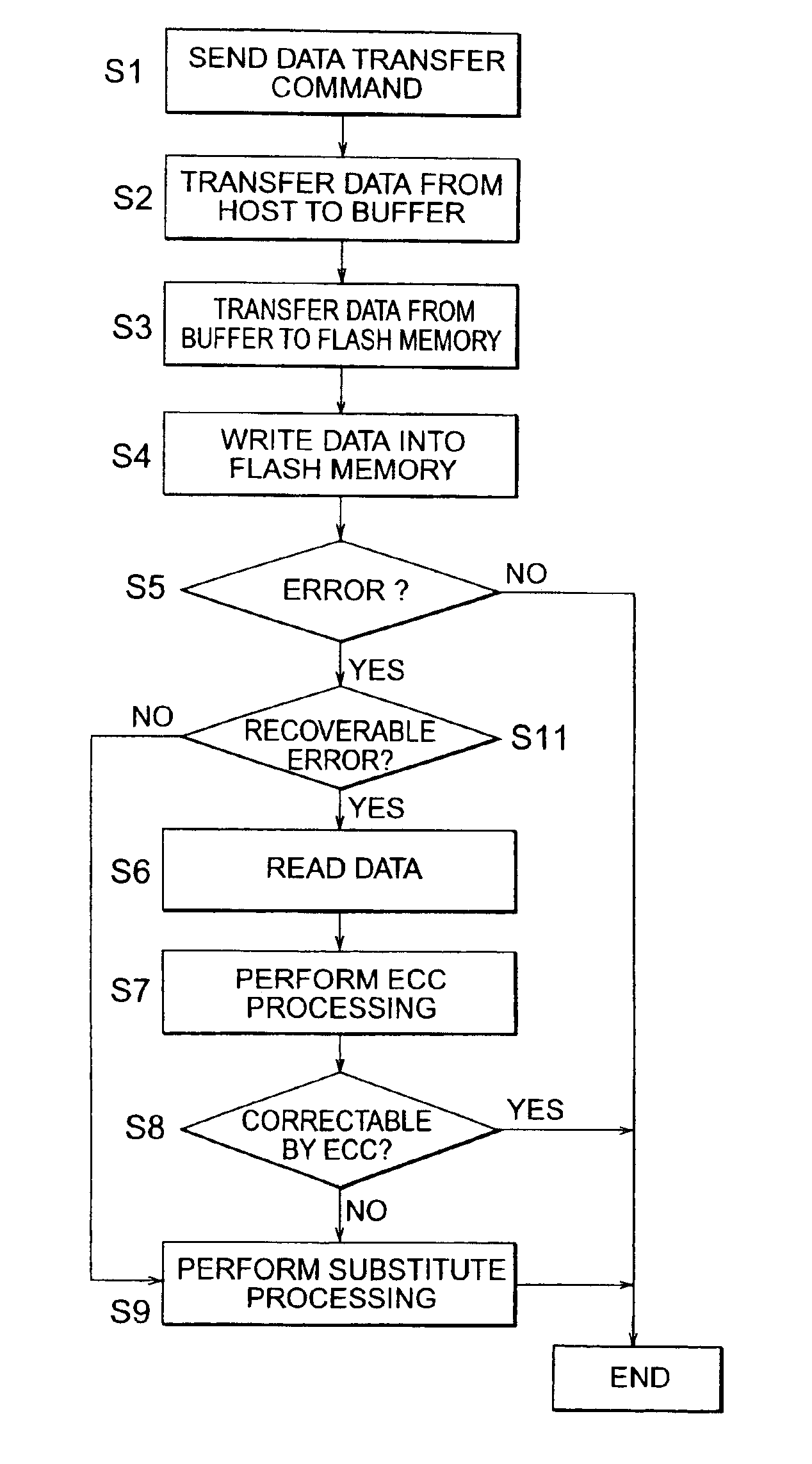
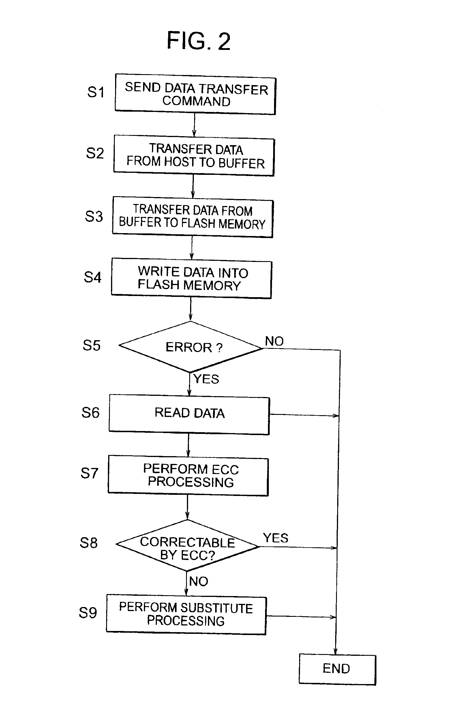
[0037]write processing that is used when the present invention is applied to the memory card with the configuration described above will be described with reference to the flowchart in FIG. 2.

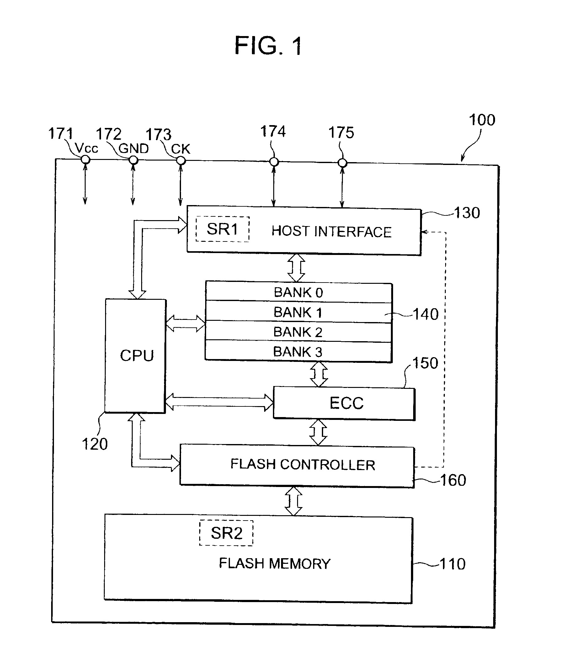
[0038]When writing data in the memory card in the first embodiment of write processing, a data transfer command is first sent from an external host CPU to the memory card (step S1). Then, write data is transferred from the host CPU to the memory card. The transferred command is supplied to the microprocessor 120 via the interface 130, and the transferred data is stored in the buffer memory 140 via the interface 130 (step S2). The command and the data described above are transferred serially. A write address is sent with the command.

[0039]After write data is transferred in a predetermined manner, the write data is then transferred from the buffer memory 140 to the flash memory 110 (step S3). The data is transferred in parallel, eight bits at a time. At this time, the write data is transferred vi...

second embodiment

[0044]Next, write processing that is used when the present invention is applied to the memory card in FIG. 1 will be described with reference to the flowchart in FIG. 3. This embodiment may be used when the status register SR2 in the flash memory 110 has the following flags: a flag indicating that a general write error has occurred when there is a bit whose threshold voltage does not reach a predetermined level at write time and a flag indicating that a recoverable error, such as an excessive write error, has occurred when there is a bit whose threshold voltage exceeds a predetermined level at write time.

[0045]Write processing in this embodiment is almost the same as that of the first embodiment in FIG. 2. The only difference is step S11 that follows step S5 in the flowchart in FIG. 2. In this step, the flag in status register SR2 are checked to determine whether to correct an error with the error correction circuit. In step S11, the excessive write error flag is checked to see if t...

third embodiment

[0048]Next, write processing that is used when the present invention is applied to the memory card in FIG. 1 will be described with reference to the flowchart in FIG. 4. This embodiment includes recovery processing for a so-called retention defect bit that is generated when the threshold voltage is out of a predetermined range because data has not been rewritten for a long time.

[0049]A part of write processing in this embodiment is the same as that of write processing in the first embodiment shown in FIG. 2. The only difference is retention defect recovery processing in steps S21-S23 that are inserted between steps S8 and S9 in the flowchart in FIG. 2.

[0050]More specifically, when the error correction circuit has judged that it can correct the error in step 8, a check is made in the next step, S21, if the number of errors is smaller than a predetermined number n (for example, 2). If so, the write operation is ended immediately. On the other hand, if the number of errors is larger th...


PUM


Abstract

When a non-volatile memory write error occurs in a card storage device containing a non-volatile memory and an error correction circuit, write data is read from the non-volatile memory and a check is made if the error can be corrected by the error correction circuit. If the error can be corrected, the write operation is ended. If the error correction circuit cannot correct the error, substitute processing is performed to write data into some other area.

Description

CROSS-REFERENCE TO RELATED APPLICATION[0001]This application is a continuation of Application No. 10 / 078,471 filed Feb. 21, 2002 now U.S. Pat. No. 6,608,784.BACKGROUND OF THE INVENTION[0002]The present invention relates to a technology that may be applied to a non-volatile storage device, for example, to a technology that may be applied to a non-volatile semiconductor memory such as a flash memory or a card storage device such as a multimedia card or a smart media memory card.[0003]Recently, a card storage device, called a memory card containing a non-volatile memory, such as a flash memory, that retains its storage data even after the power has been switched off, is widely used as a data storage medium for portable electronic apparatus such as a digital camera.[0004]As compared with a volatile memory such as a RAM, a non-volatile memory varies widely in its memory device characteristics. At the same time, a non-volatile memory is not designed basically for repeated write operation....

Claims


Application Information

Patent Timeline
IPC IPC(8): G11C29/00G06F11/00G06F12/16G06F11/10G11C16/06G11C29/42
CPCG06F11/1068G11C16/3431G11C29/76G11C29/765G11C29/81G11C29/82G11C16/04G11C2029/0411
Inventor KANAMORI, MOTOKIKATAYAMA, KUNIHIROSHIRAISHI, ATSUSHIKURAKATA, SHIGEOSHIKATA, ATSUSHI
Owner RENESAS ELECTRONICS CORP
Why Eureka
Try Eureka