Stack chip package structure

Active Publication Date: 2005-07-19
VIA TECH INC
View PDF8 Cites 10 Cited by
  • Summary
  • Abstract
  • Description
  • Claims
  • Application Information

AI Technical Summary

Benefits of technology

[0010]Accordingly, one object of the present invention is to provide a stack chip package structure with a die and a thermal conductive block therein such that stress concentration at the bottom

Problems solved by technology

Hence, a compact IC chip will produce a lot of heat during operation leading to an increase in temperature.
As temperature of the IC chip rises to a level above the normal operating temperature, co

Method used


Image

  • Stack chip package structure
  • Stack chip package structure
  • Stack chip package structure

Examples


Embodiment Construction

[0024]Reference will now be made in detail to the present preferred embodiments of the invention, examples of which are illustrated in the accompanying drawings. Wherever possible, the same reference numbers are used in the drawings and the description to refer to the same or like parts.

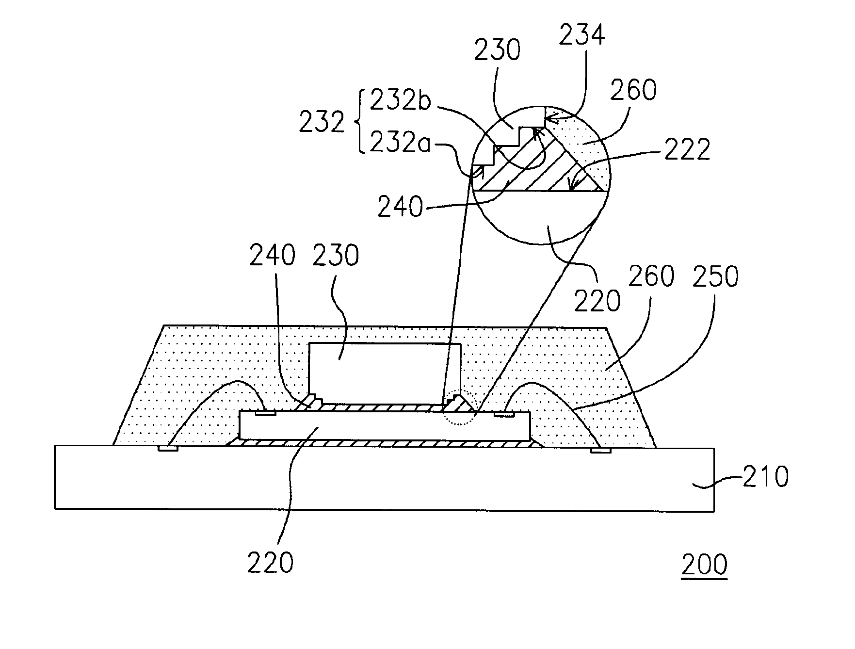
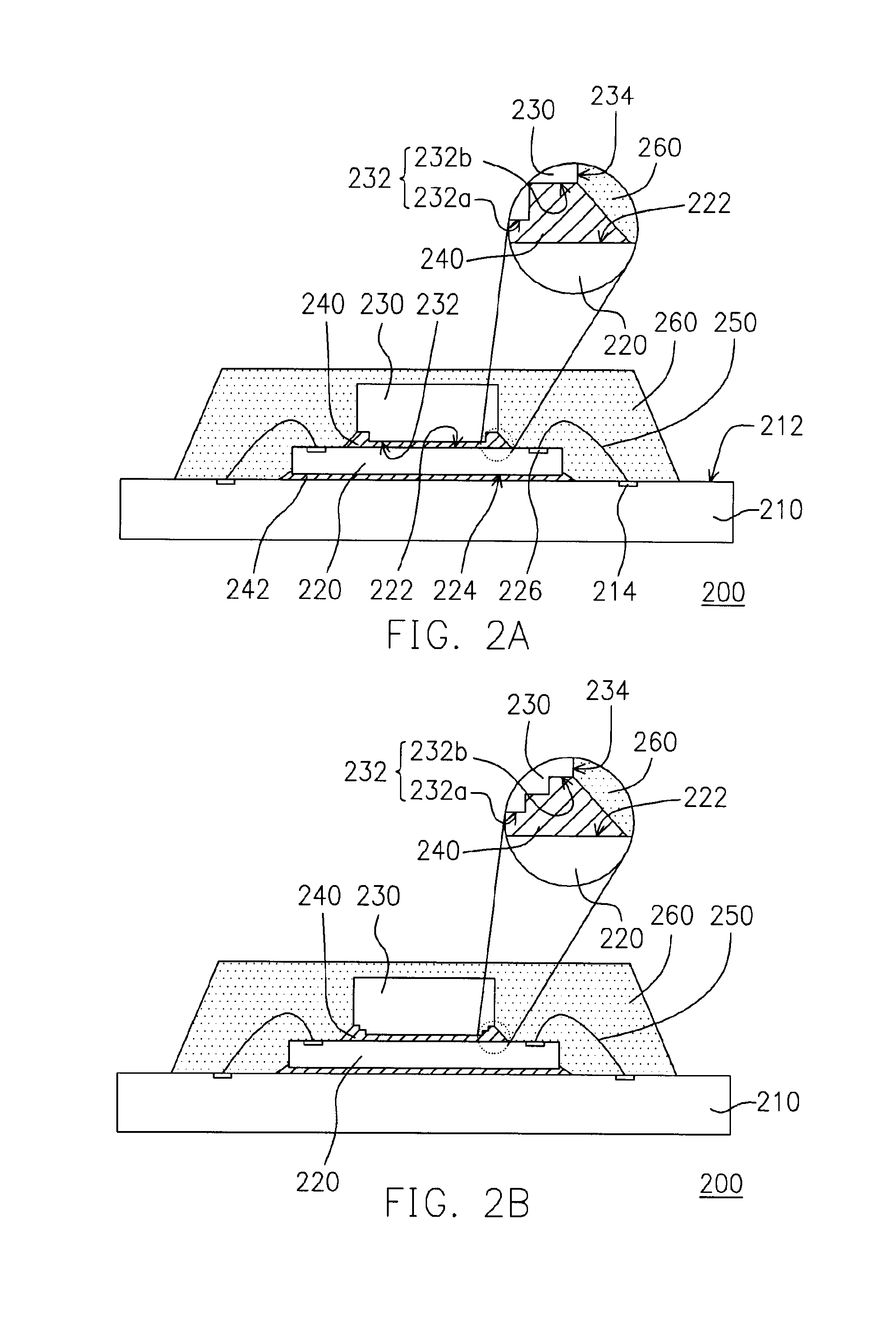
[0025]FIG. 2A is a schematic cross-sectional view of a stack chip package structure according to a first preferred embodiment of this invention, wherein the peripheral surfaces of the thermal conductive block are single ladder surfaces. As shown in FIG. 2A, the chip package structure 200 mainly includes a carrier 210, a die 220, a thermal conductive block 230, a adhesive layer 240, a plurality of conductive wires 250 and a molding compound 260. The carrier 210 is, for example, a substrate or a lead frame (here, the carrier 210 is a substrate). The carrier 210 has a carrier surface 212 and a plurality of bonding pads 214 thereon. The die 220 has an active surface 222 and a back surface 224. The back s...


PUM


Abstract

A stack chip package structure is provided. One principal feature of the structure is the formation of a few peripheral surfaces (e.g. ladder or lead-angle surfaces) at the bottom peripheral sections of a stack structure. When the stack structure is attached to a surface of a die through an adhesive layer, the thickness of the adhesive layer under a peripheral section of the stack structure is greater than a central region. Therefore, as the chip package is subjected to a thermal stress test, the adhesive layer under the peripheral sections of the stack structure is able to provide some buffering against thermal stress so that the stress concentration around the stack structure is reduced. Consequently, damages of the die surface due to stress are prevented and the average working life of the chip package is extended.

Description

CROSS REFERENCE TO RELATED APPLICATIONS[0001]This application claims the priority benefit of Taiwan application serial no. 92201153, filed on Jan. 22, 2003.BACKGROUND OF INVENTION[0002]1. Field of Invention[0003]The present invention relates to a chip package structure. More particularly, the present invention relates to a stack chip package structure.[0004]2. Description of Related Art[0005]As techniques for fabricating a smaller integrated circuit (IC) progresses, the level of integration inside an IC chip also increases. Moreover, the number of transistors inside the IC chip increases and the cross-sectional area of internal conductive lines are reduced. In general, heat is produced in each transistor and conductive line. Hence, a compact IC chip will produce a lot of heat during operation leading to an increase in temperature. As temperature of the IC chip rises to a level above the normal operating temperature, computational errors, temporary malfunction or permanent damages ma...

Claims


Application Information

Patent Timeline
IPC IPC(8): H01L23/373H01L25/065H01L23/28H01L23/31H01L23/433H01L23/34H01L29/06
CPCH01L23/3128H01L23/3737H01L23/4334H01L24/32H01L24/33H01L25/0657H01L29/0657H01L2224/27013H01L2224/32145H01L2224/32225H01L2224/48091H01L2224/48227H01L2224/48247H01L2224/73265H01L2224/83051H01L2225/0651H01L2225/06513H01L2225/06555H01L2225/06575H01L2225/06582H01L2924/01005H01L2924/01074H01L2924/01082H01L2924/14H01L2924/3011H01L2924/00014H01L24/48H01L2924/01033H01L2224/32245H01L2224/16245H01L2224/26145H01L2924/00H01L2924/3512H01L2924/00012H01L2924/10155H01L2224/83385H01L2224/451H01L2924/351H01L2924/181H01L24/45H01L24/73H01L2924/00015
Inventor LEE, I-TSENGLIAO, HSUEH KUOTSENG, JEN-TE
Owner VIA TECH INC
Why Eureka
Try Eureka