High pressure processing chamber for semiconductor substrate

a processing chamber and semiconductor substrate technology, applied in the direction of coatings, chemical vapor deposition coatings, chemical apparatus and processes, etc., can solve the problems that the high pressure processing chambers of existing supercritical processing systems are not appropriate to meet the unique needs of processing semiconductor substrates

Inactive Publication Date: 2005-07-26
TOKYO ELECTRON LTD
View PDF231 Cites 42 Cited by
  • Summary
  • Abstract
  • Description
  • Claims
  • Application Information

AI Technical Summary

Problems solved by technology

Processing of semiconductor substrates presents unique problems not associated with processing of other workpieces.
However, recent advancements for the integrated circuits include etch feature critical dimensions below dimensions with sufficient structure to withstand the stripper bath and low dielectric constant materials which cannot withstand an oxygen environment of the plasma ashing.
However, high pressure processing chambers of existing supercritical processing systems are not appropriate to meet the unique needs of the semiconductor processing requirements.

Method used


Image

  • High pressure processing chamber for semiconductor substrate
  • High pressure processing chamber for semiconductor substrate
  • High pressure processing chamber for semiconductor substrate

Examples


Embodiment Construction

[0021]The preferred pressure chamber of the present invention is preferably used for supercritical processing of a semiconductor wafer. Preferably, the preferred pressure chamber forms part of a supercritical processing module. Preferably, the supercritical processing module is used to remove photoresist from the semiconductor wafer. Alternatively, the supercritical processing module is used for other supercritical processing of the semiconductor wafer, such as photoresist development.

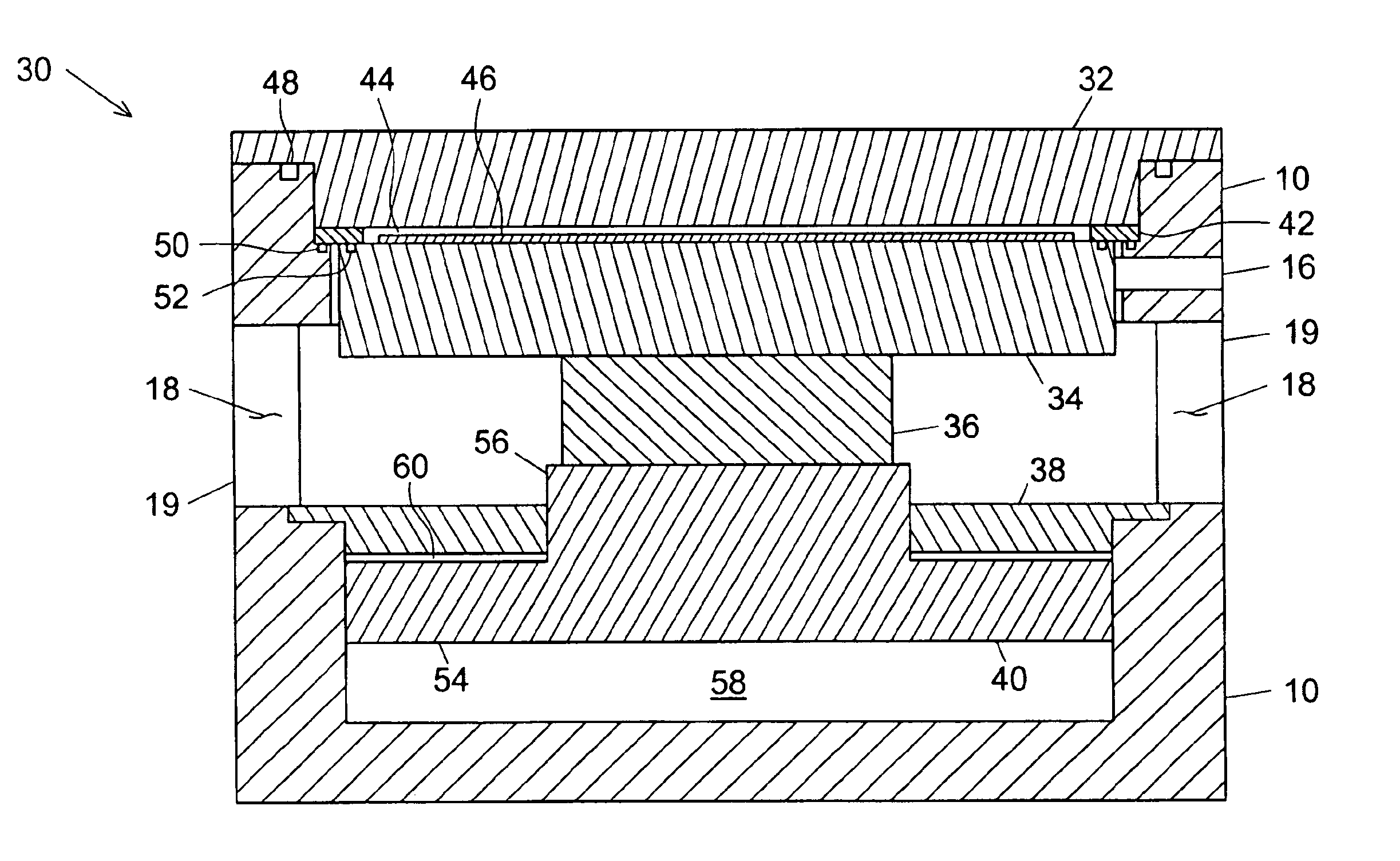
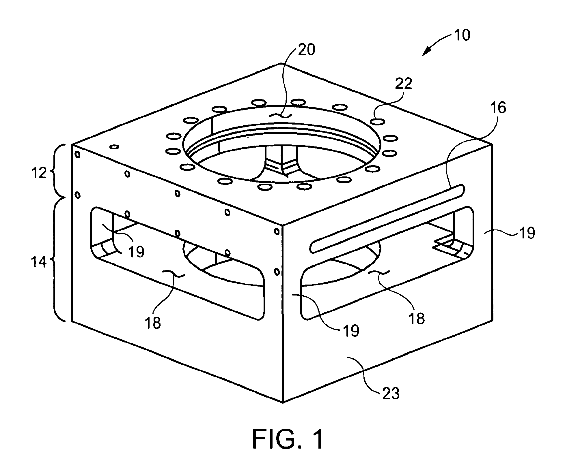
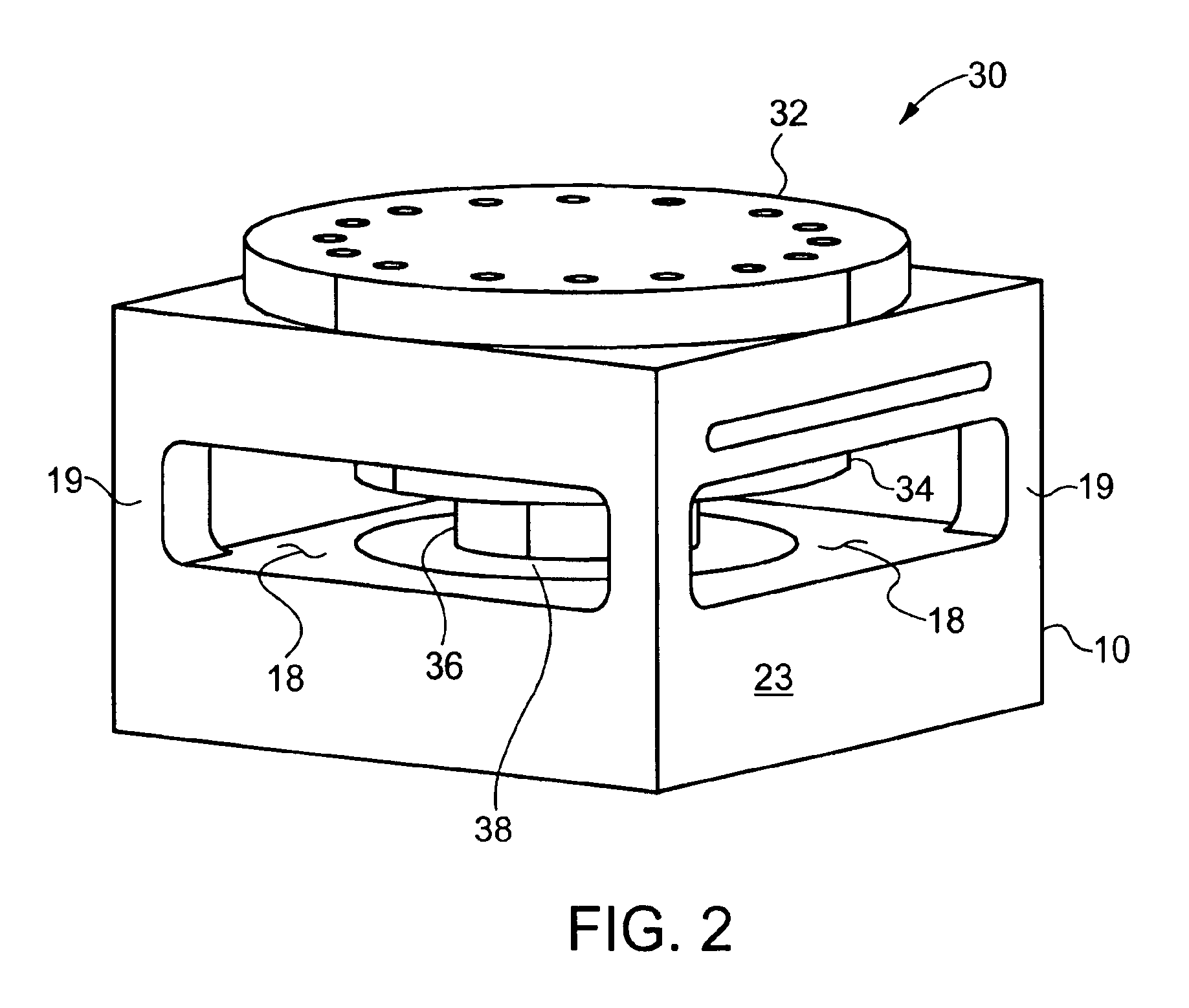
[0022]A pressure chamber frame of the present invention is illustrated in FIG. 1. The pressure chamber frame 10 includes a pressure chamber housing portion 12, an opening / closing housing portion 14, a wafer slit 16, windows 18, posts 19, a top opening 20, and top bolt holes 22. The wafer slit 16 is preferably sized for a 300 mm wafer. Alternatively, the wafer slit 16 is sized for a larger or a smaller wafer. Further alternatively, the wafer slit 16 is sized for a semiconductor substrate other than a wa...


PUM


Abstract

A high pressure chamber comprises a chamber housing, a platen, and a mechanical drive mechanism. The chamber housing comprises a first sealing surface. The platen comprises a region for holding the semiconductor substrate and a second sealing surface. The mechanical drive mechanism couples the platen to the chamber housing. In operation, the mechanical drive mechanism separates the platen from the chamber housing for loading of the semiconductor substrate. In further operation, the mechanical drive mechanism causes the second sealing surface of the platen and the first sealing surface of the chamber housing to form a high pressure processing chamber around the semiconductor substrate.

Description

RELATED APPLICATIONS[0001]This application claims priority from U.S. Provisional Patent Application No. 60 / 220,883, filed on Jul. 26, 2000, and from U.S. Provisional Patent Application No. 60 / 283,132, filed on Apr. 10, 2001, which are incorporated by reference.FIELD OF THE INVENTION[0002]This invention relates to the field of high pressure processing. More particularly, this invention relates to the field of high pressure processing of a semiconductor substrate.BACKGROUND OF THE INVENTION[0003]Processing of semiconductor substrates presents unique problems not associated with processing of other workpieces. Typically, the semiconductor processing begins with a silicon wafer. The semiconductor processing starts with doping of the silicon wafer to generate transistor semiconductors. Next, the semiconductor processing continues with deposition of metal and dielectric layers interspersed with etching of lines and vias to produce transistor contacts and interconnect structures. Ultimatel...

Claims


Application Information

Patent Timeline
Patent Type & Authority Patents(United States)
IPC IPC(8): H01L21/00H01L21/304H01L21/027
CPCH01L21/67051H01L21/67126H01L21/67748H01L21/67751H01L21/00
Inventor BIBERGER, MAXIMILIAN A.LAYMAN, FREDERICK PAULSUTTON, THOMAS ROBERT
Owner TOKYO ELECTRON LTD
Why Eureka
Try Eureka