Device and method for determining the orientation of a crystallographic plane in relation to a crystal surface and device for cutting a single crystal in a cutting machine

a technology of crystallographic plane and cutting machine, which is applied in the direction of stone-like material working apparatus, instruments, electrical apparatus, etc., can solve the problems of inability to eliminate possible errors upon insertion of the tilting device together with the crystal in the wire sawing apparatus, inability to measure and reorient, and inability to correct by remeasuring and reorientation. , to achieve the effect of improving the quality of the wafer, and reducing the number of cuts

Inactive Publication Date: 2005-08-02
FREIBERGER COMPOUND MATERIALS
View PDF25 Cites 12 Cited by
  • Summary
  • Abstract
  • Description
  • Claims
  • Application Information

AI Technical Summary

Benefits of technology

[0036]the angular position of a given crystallographic direction (K) of the single crystal in the cutting plane is adjusted in such a way that during cutting of the single crystal the forces acting on the cutting device are minimised.
[0037]The method and the apparatus have the advantage that the quality of the wafers is increased and that higher feed rates during cutting are made possible. Due to the improved quality of the wafers produced, further processing steps which are otherwise commonplace can be largely eliminated. Further, the precision of orientation can be increased.

Problems solved by technology

With the known method of wire sawing, such correction by remeasuring and reorientation is not possible, because all the wafers are cut from a single crystal simultaneously.
With this method, however, errors due to contamination of the stop and reference faces as well as adhesion errors which arise when the single crystal is stuck to the work piece substrate are not detected, as orientation measurement takes place outside the machine.
Possible errors upon insertion of the tilting device together with the crystal in the wire sawing apparatus therefore likewise cannot be eliminated, however.

Method used


Image

  • Device and method for determining the orientation of a crystallographic plane in relation to a crystal surface and device for cutting a single crystal in a cutting machine
  • Device and method for determining the orientation of a crystallographic plane in relation to a crystal surface and device for cutting a single crystal in a cutting machine
  • Device and method for determining the orientation of a crystallographic plane in relation to a crystal surface and device for cutting a single crystal in a cutting machine

Examples


Embodiment Construction

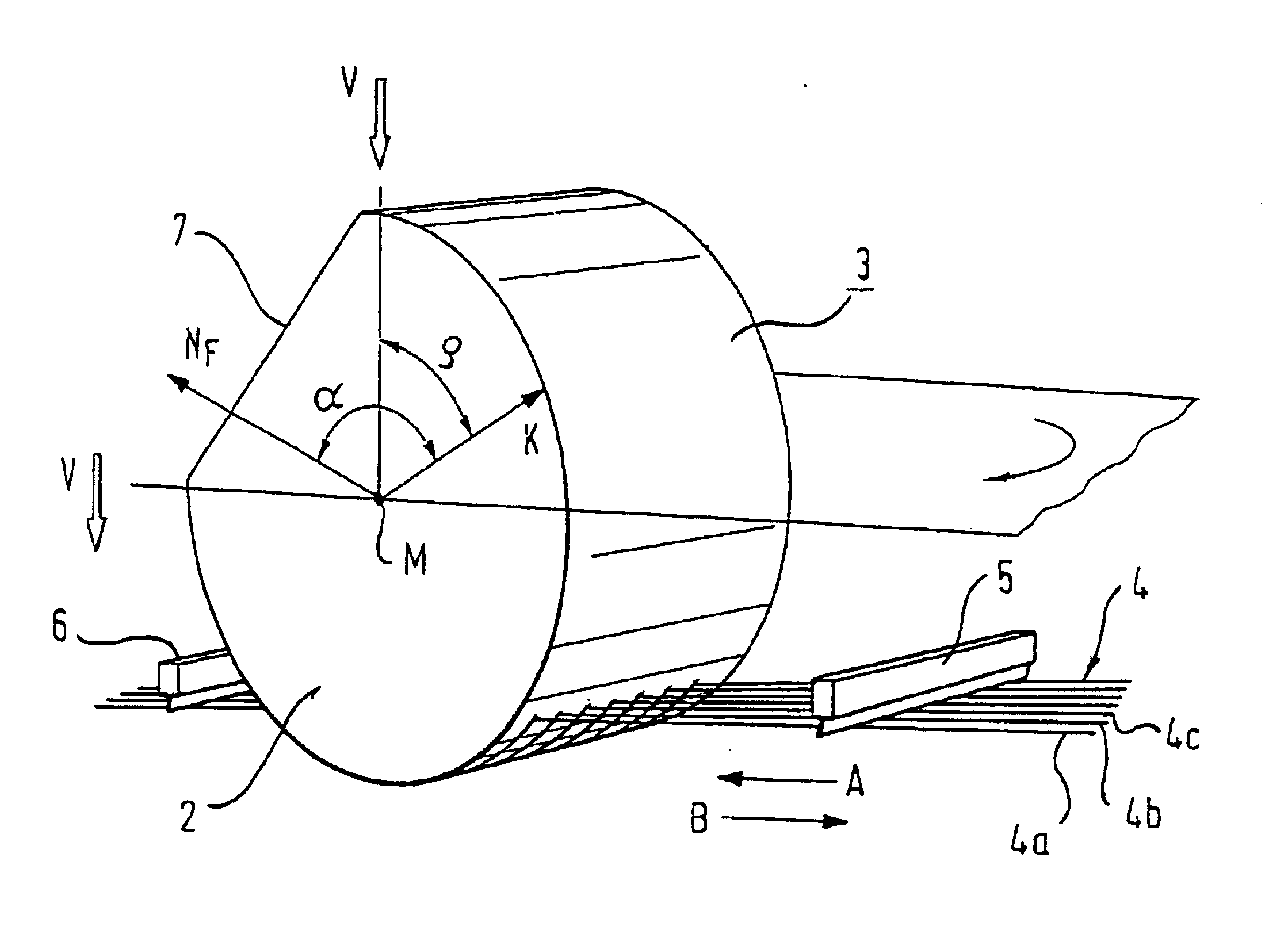
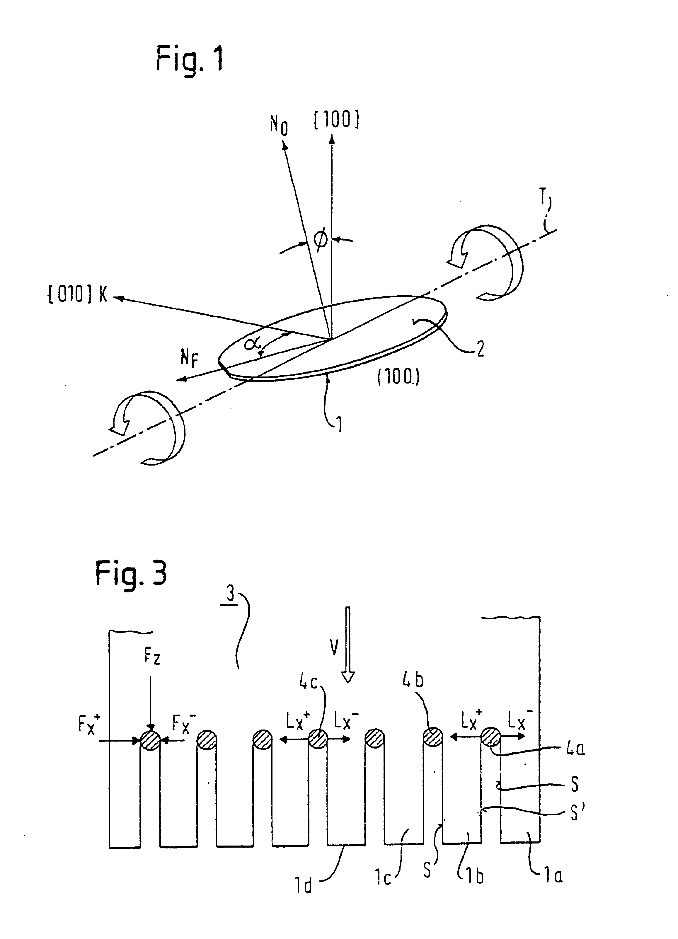
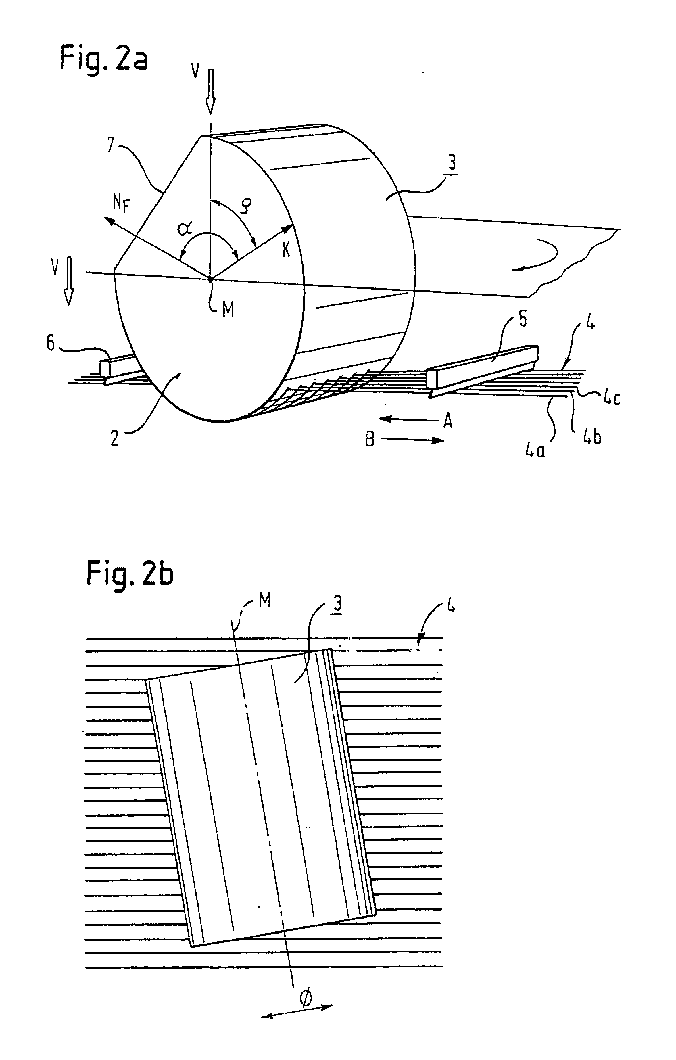
[0049]For a better understanding, first the forces acting on the wafer during wire sawing are described below with the aid of FIGS. 1 to 4. As can be seen from FIG. 3, during wire sawing the wires 4a, 4b, 4c penetrate into the single crystal 3 for cutting off wafers 1a, 1b, 1c, etc. During the cutting operation, after reaching a critical depth of penetration into the single crystal 3 the diamond particles of the wires produce microcracks which lead to removal of material due to mutual crosslinking. This critical depth of penetration depends on the orientation of a given crystallographic direction K located in the wafer surface 2, for example the [010] direction, relative to the feed direction V, which is explained below.

[0050]As can be seen from FIGS. 1 and 2a, the single crystal 3 exhibits an orientation feature in the form of a plane outer-surface section 7, the so-called flat, which has been applied in a given manner after growing the single crystal 1 in such a way that an angle ...


PUM

PropertyMeasurementUnit
angle measuringaaaaaaaaaa
angleaaaaaaaaaa
partial pressureaaaaaaaaaa

Abstract

An apparatus and a method for determining the orientation of a crystallographic plane (100) relative to a crystal surface (2) are provided, in which the orientation is free from errors of adhesion of the crystal or contamination of the holders for the crystal. For this purpose, the angle which the crystal surface to be measured forms with a reference axis and the angle which the crystallographic plane forms with the reference axis are measured and subtracted. In a wire sawing apparatus with an X-Y positioning unit, next the desired correction is made with the aid of measurement of the orientation and at the same time the crystal is displaced in horizontal and vertical positions. As a result, there remains a further degree of freedom of rotation of the crystal in the cutting plane for achieving a cut which is free from forces perpendicular to the feed direction and wire direction, so that no tool deflection takes place or the cutting forces are minimal. Further, the precision of orientation is increased.

Description

CROSS-REFERENCE TO RELATED APPLICATIONS[0001]Not applicableSTATEMENT REGARDING FEDERALLY SPONSORED RESEARCH OR DEVELOPMENT[0002]Not applicableINCORPORATION-BY-REFERENCE OF MATERIAL SUBMITTED ON A COMPACT DISC[0003]Not ApplicableBACKGROUND OF THE INVENTION[0004](1) Field of the Invention[0005]The invention concerns an apparatus and a method for determining the orientation of a crystallographic plane relative to a crystal surface as well as an apparatus and a method for cutting a single crystal in a cutting machine.[0006](2) Description of Related Art[0007]For certain applications, semiconductor wafers with so-called misorientation are needed. As can be seen from FIG. 1, in a semiconductor wafer 1 with misorientation a certain crystallographic plane, e.g. the (100) plane, is not parallel to the wafer surface 2. The angle of misorientation φ is in this case the angle which the vector [100] which is perpendicular to the (100) plane forms with the normal vector N0 which is perpendicular ...

Claims


Application Information

Patent Timeline
Patent Type & Authority Patents(United States)
IPC IPC(8): B28D5/04B28D5/00G01N23/20H01L21/304
CPCB28D5/0088G01N23/20016B28D5/045
Inventor HAMMER, RALFGRUSZYNSKY, RALFKLEINWECHTER, ANDREFLADE, TILO
Owner FREIBERGER COMPOUND MATERIALS
Why Eureka
Try Eureka