Semiconductor device having a boosting circuit to suppress current consumption

a technology of boosting circuit and circuit, which is applied in the direction of pulse generator, pulse technique, instruments, etc., can solve the problems of large ripple of power supply voltage, deterioration of response of circuit, etc., and achieve the effect of reducing current consumption

Inactive Publication Date: 2005-08-09
RENESAS ELECTRONICS CORP
View PDF4 Cites 49 Cited by
  • Summary
  • Abstract
  • Description
  • Claims
  • Application Information

AI Technical Summary

Benefits of technology

[0010]The present invention is directed to solve the above problem, and has as its object to provide a semiconductor device having a boosting circuit achieving a boosting operation with a small variation in voltage while suppressing a current consumption in a standby state.
[0012]According to the present invention, provided can be a boosting circuit which can supply an internal power supply voltage including a small amount of ripple with a reduced current consumption in a standby state in a semiconductor device.

Problems solved by technology

However, the response of the circuit is deteriorated when the DC current is reduced, resulting in a practical problem.
For this reason, the low response of the boosting circuit also boosts a high voltage in the operation of the charge pump circuit, resulting in a large amount of ripple of a power supply voltage.

Method used


Image

  • Semiconductor device having a boosting circuit to suppress current consumption
  • Semiconductor device having a boosting circuit to suppress current consumption
  • Semiconductor device having a boosting circuit to suppress current consumption

Examples


first embodiment

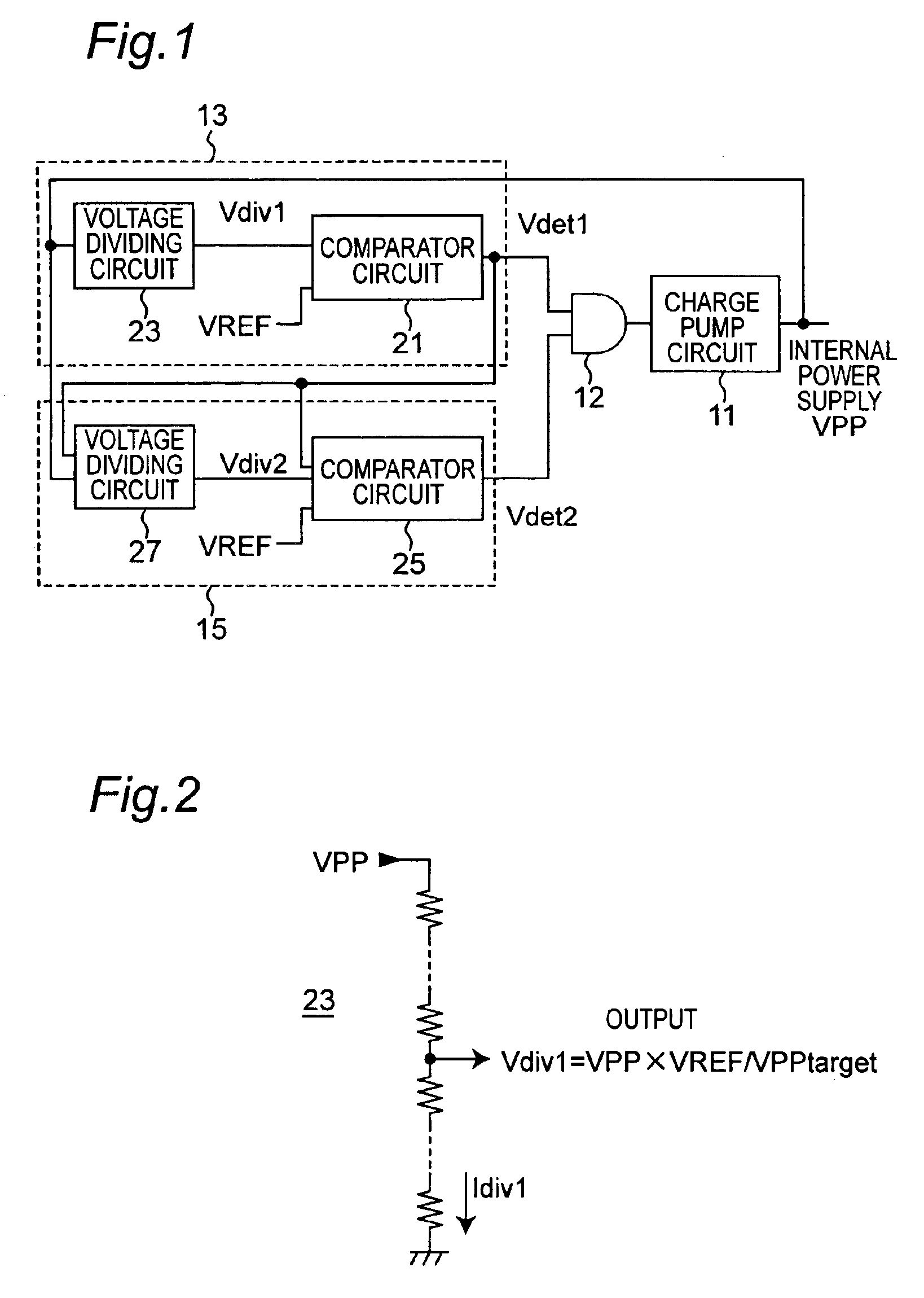
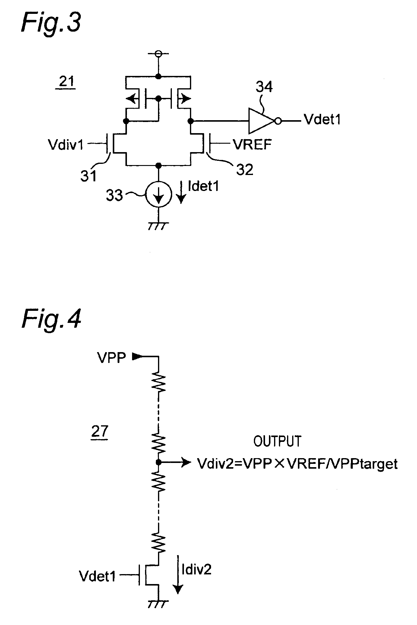
[0024]FIG. 1 is a diagram showing the configuration of a boosting circuit included in a semiconductor device according to the present invention. This boosting circuit is a circuit for generating an internal power supply voltage at a standby state of the semiconductor device, and outputs a voltage which is obtained by boosting a voltage supplied from external or a dropped voltage supplied from external. The boosting circuit includes a charge pump circuit 11 for supplying an internal power supply voltage of the semiconductor device, and first and second detection circuits 13 and 15 for detecting an output voltage from the charge pump circuit 11. The boosting circuit further includes an AND gate 12 for performing AND operation of outputs Vdet1 and Vdet2 from the first and second detection circuits 13 and 15. The charge pump circuit 11 is activated on the basis of the result of AND operation of outputs Vdet1 and Vdet2 of the first and second detection circuits 13 and 15. The second dete...

second embodiment

[0040]Another example of the boosting circuit will be described below. The configuration of this embodiment is basically the same as that of the first embodiment. However, the second embodiment is different from the first embodiment in that the detection level of the second detection circuit is made different from the detection level of the first detection circuit by a predetermined value Δ. More specifically, as shown in FIG. 7, the resistances of the resistors in a voltage dividing circuit 27b of the second detection circuit of this embodiment are set so as to output an output voltage Vdiv2 obtained by the following equation.

Vdiv2=Vpp·VREF / (Vpptarget+Δ)

[0041]An operation of the boosting circuit will be described below with reference to FIG. 8.

[0042]During a period in which the internal power supply voltage Vpp is higher than a target voltage Vpptarget, both the first and second detection circuits 13 and 15 output signals at “Low” level. When the internal power supply voltage Vpp g...

third embodiment

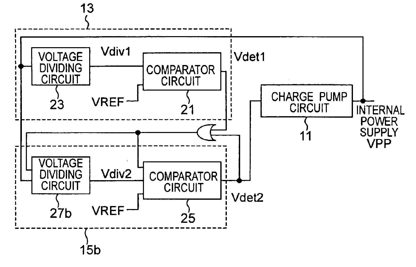
[0048]Still another example of a boosting circuit included in the semiconductor device according to the present invention will be described below. FIG. 9 shows the configuration of the boosting circuit. In the boosting circuit according to this embodiment, the charge pump circuit 11 is activated / inactivated on the basis of only an output of a second detection circuit 15b.

[0049]The second detection circuit 15b is the same circuit as described in the second embodiment, including a voltage dividing circuit 27b having a detection level different from that of the first detection circuit. A voltage obtained by performing an OR operation of the output Vdet1 of the first detection circuit 13 and the output Vdet2 of the second detection circuit 15b is input to the second detection circuit 15b. The second detection circuit 15b is activated based on the voltage obtained by the OR operation.

[0050]FIG. 10 is a diagram showing an operation of the boosting circuit according to this embodiment. Th...


PUM


Abstract

A semiconductor device includes a boosting circuit for supplying a power supply voltage during a standby state of the semiconductor device. The boosting circuit includes a charge pump circuit and first and second detection circuits for detecting an output voltage of the charge pump circuit. The second detection circuit is operated by a DC current greater than that of the first detection circuit, and is activated by an output (Vdet1) from the first detection circuit. The charge pump circuit is activated based on at least an output (Vdet2) from the second detection circuit.

Description

BACKGROUND OF THE INVENTION[0001]1. Field of the Invention[0002]The present invention relates to control of a boosting circuit which generates an internal power supply voltage in a semiconductor device.[0003]2. Related Art[0004]In a semiconductor device, a circuit for generating a desired voltage in the semiconductor device, a charge pump circuit is known. A semiconductor device such as a FLASH MEMORY includes two internal voltage generation circuits which operate in a normal operation state and a standby state to reduce a standby current.[0005]An internal voltage generation circuit in the semiconductor device is for example disclosed in Reference 1* and Reference 2**. These patent documents disclose a boosting circuit comprising a charge pump circuit and a circuit for detecting an output voltage of the charge pump circuit to control an operation of the charge pump based on the detected output voltage. More specifically, the following technique is disclosed. That is, the boosting ci...

Claims


Application Information

Patent Timeline
Patent Type & Authority Patents(United States)
IPC IPC(8): H02M3/07H02M3/04H03K17/30H01L27/04H01L21/822
CPCH02M3/073H03K17/302
Inventor SENDA, MINORU
Owner RENESAS ELECTRONICS CORP
Why Eureka
Try Eureka