Transparent electrode, electronic device, and organic electroluminescent element

Inactive Publication Date: 2015-10-08
KONICA MINOLTA INC
View PDF2 Cites 4 Cited by
  • Summary
  • Abstract
  • Description
  • Claims
  • Application Information

AI Technical Summary

Benefits of technology

The present invention provides a transparent electrode with high transparency, low sheet resistance and small variation in resistance during high temperature storage. Additionally, the invention offers an electronic device and an organic electroluminescent element with the transparent electrode, which have excellent optical transparency, low driving voltage and small voltage variation under constant current. The transparent electrode has a conductive layer containing silver and an intermediate layer containing an organic compound containing a sulfur atom(s) having an unshared electron pair). The silver atoms and the organic compound containing a sulfur atom(s) react with each other, resulting in reduced diffusion distance of the silver atoms, which prevents the formation of silver islands and promotes the growth of a single-layer nucleus.

Problems solved by technology

However, because ITO uses a rare metal, indium, material costs are high, and also annealing at about 300° C. is needed after its deposition in order to reduce resistance.
However, the art to make a thin film with an alloy of silver and Mg has problems, for example, that resistance of the obtained thin film is about 100Ω / □, which is insufficient, and that deterioration over time is significant because Mg is easily oxidized.
Further, the art to make a thin film with Zn or Sn as a starting material has problems, for example, that a sufficient resistance cannot be obtained, that a ZnO thin film containing Zn reacts with water, whereby its properties easily change, and that an SnO2 thin film containing Sn is difficult to process by etching.
However, in the case of Patent Document 5, because the deposited layer of silver is thick, optical transparency (degree of transparency) is bad.
However, when the deposited layer of silver, which easily causes migration, is made to be thinner, the sheet resistance is high and the sheet resistance variation in high temperature storage is large, so that electrode characteristics cannot be maintained.
Consequently, an OLED using such an electrode has problems that driving voltage is high and voltage variation under constant current is large.

Method used


Image

  • Transparent electrode, electronic device, and organic electroluminescent element
  • Transparent electrode, electronic device, and organic electroluminescent element
  • Transparent electrode, electronic device, and organic electroluminescent element

Examples


examples

[0371]Hereinafter, the present invention is detailed with Examples. However, the present invention is not limited thereto. Note that “%” used in Examples stands for “mass % (percent by mass)” unless otherwise specified.

[0372]>

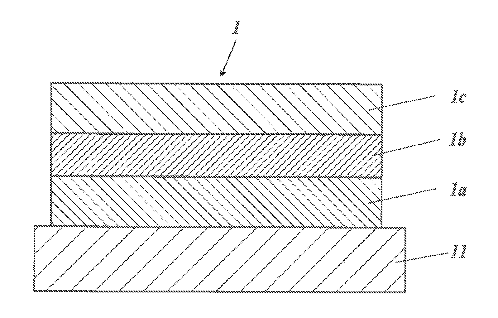
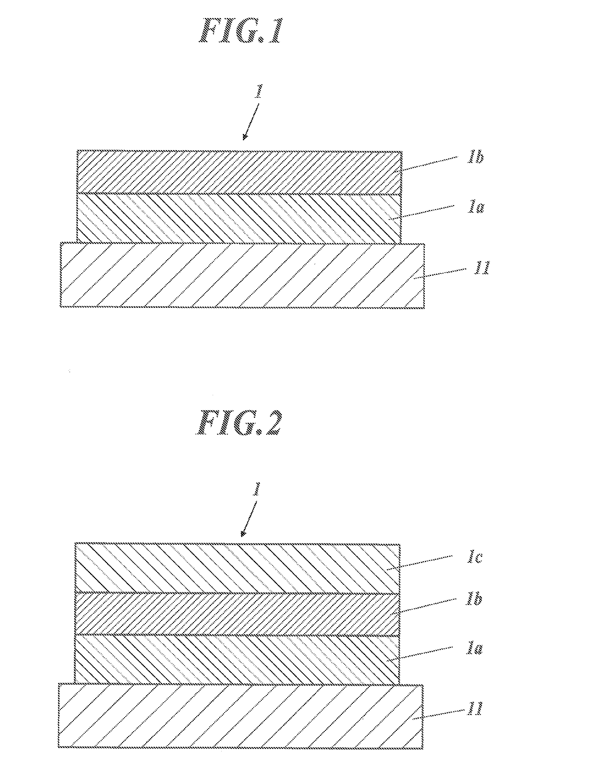
[0373]By the method described below, transparent electrodes 1 to 63 were each produced in such a way that the area of a conductive region was 5 cm×5 cm. The transparent electrodes 1 to 4 were each produced as a transparent electrode having a single-layer structure, and the transparent electrodes 5 to 63 were each produced as a transparent electrode having a multilayer structure of an intermediate layer(s) and a conductive layer.

[0374][Production of Transparent Electrode 1]

[0375]By the method described below, the transparent electrode 1 having a single-layer structure was produced as a comparative example.

[0376]A base composed of transparent alkali-free glass was fixed to a base holder of a commercial vacuum deposition device, and the base holder was mounted in ...

second example

Production of Luminescent Panels

[0414][Production of Luminescent Panel 1]

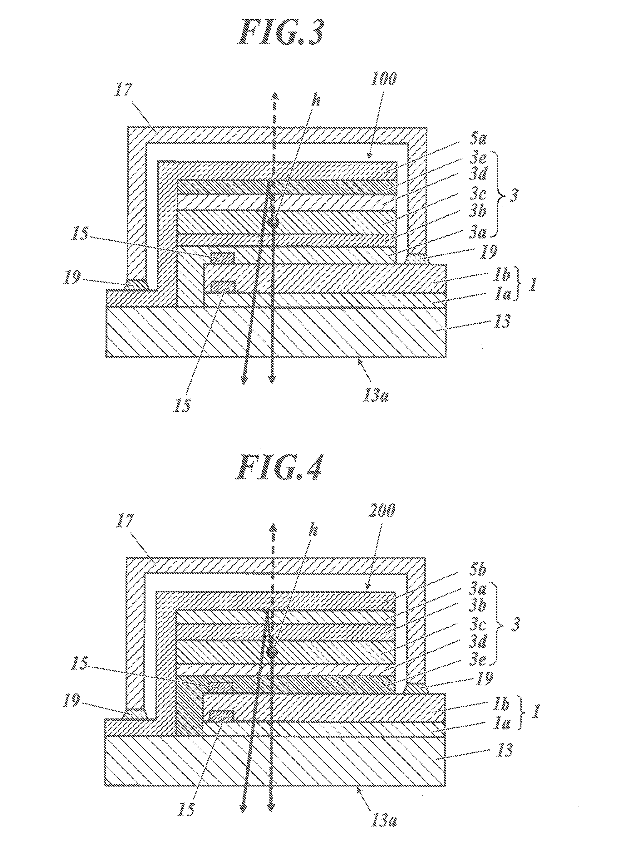
[0415]A top-and-bottom emission type luminescent panel 1 having the structure (but having no intermediate layer 1a) shown in FIG. 7 was produced through the procedure described below by using, as an anode, the transparent electrode 1 produced in First Example.

[0416]First, a transparent substrate 13 having the transparent electrode 1 formed of only the conductive layer 1b produced in First Example was fixed to a substrate holder of a commercial vacuum deposition device, and a vapor deposition mask was disposed in such a way as to face a formation face of the transparent electrode 1 (conductive layer 1b only). Further, heating boats in the vacuum deposition device were filled with materials for respective layers constituting a light-emitting functional layer 3 at their respective amounts optimal to form the layers. The heating boats used were composed of a tungsten material for resistance heating.

[0417]Next, the ...


PUM

PropertyMeasurementUnit
Electrical resistanceaaaaaaaaaa
Nanoscale particle sizeaaaaaaaaaa
Transmittivityaaaaaaaaaa

Abstract

A transparent electrode includes a conductive layer and an intermediate layer disposed adjacent to the conductive layer. The transparent electrode has a light transmittance of 50% or more at a wavelength of 550 nm and a sheet resistance of 20Ω / □ or less. The intermediate layer contains an organic compound containing a sulfur atom having an unshared electron pair. The conductive layer is composed of silver as a main component.

Description

TECHNICAL FIELD[0001]The present invention relates to a transparent electrode, an electronic device and an organic electroluminescent element, particularly a transparent electrode having high optical transparency, low sheet resistance and small sheet resistance variation in high temperature storage, and an electronic device and an organic electroluminescent element each provided with the transparent electrode and having excellent optical transparency, low driving voltage and small voltage variation under constant current.BACKGROUND ART[0002]An organic electroluminescent element (also called an “organic EL element” or an “organic-field light-emitting element”), which utilizes electroluminescence (hereinafter abbreviated to “EL”) of an organic material, is a thin-film type completely-solid state element capable of light emission at a low voltage of about several volts to several ten volts and having many excellent characteristics; for example, high luminescence, high efficiency of lig...

Claims


Application Information

Patent Timeline
IPC IPC(8): H01L51/52
CPCY10T428/31678H01L51/5215H01L51/005H01L51/0068H01L51/0074H01L51/0067H01L51/0052H01L51/0069H01L51/007H01L51/0072H01L51/0071H01L51/0061H01L51/0058H10K85/654H10K85/656H10K85/324H10K85/6572H10K59/80517H10K50/816H10K85/60H10K85/615H10K85/626H10K85/636H10K85/655H10K85/657H10K85/6565H10K85/6576
Inventor OZEKI, HIDEKANEIIJIMA, TAKAYUKIYOSHIDA, KAZUHIROHAKII, TAKESHI
Owner KONICA MINOLTA INC
Why Eureka
Try Eureka