Circuit substrate having improved connection reliability and a method for manufacturing the same
- Summary
- Abstract
- Description
- Claims
- Application Information
AI Technical Summary
Benefits of technology
Problems solved by technology
Method used
Image

Examples
first embodiment
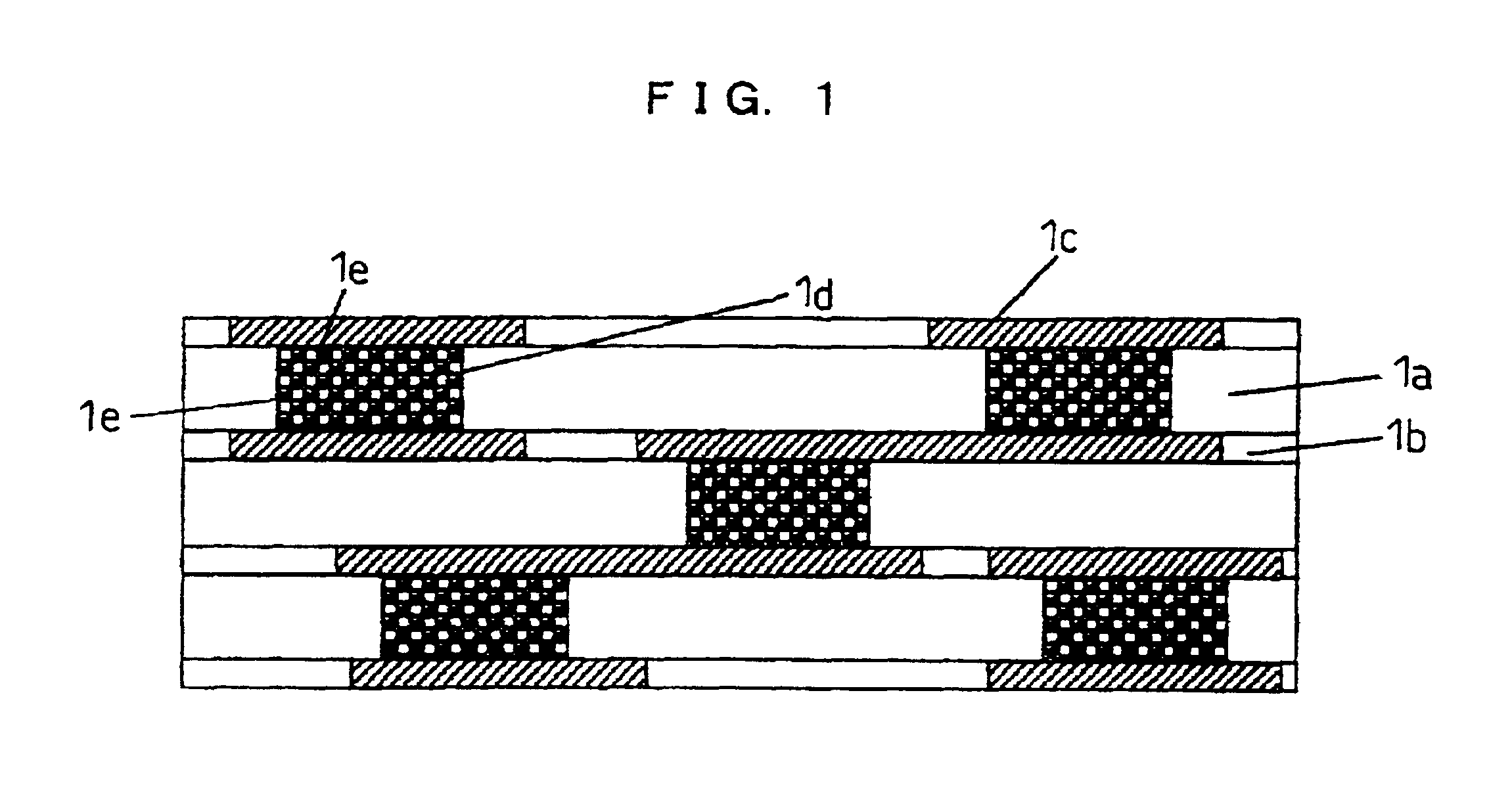
[0068]In this embodiment, an epoxy resin series adhesive having a glass transition temperature of 200° C. is prepared as the resin adhesive layer 1b to be formed on the insulating base 1a. Further, a cured product which is made from a conductive powder and an epoxy resin and which has a glass transition temperature of 180° C. is prepared as the conductive paste 1d.
[0069]This embodiment is characterized in that the glass transition temperature of the conductive adhesive layer 1b is set to be higher than the glass transition temperature of the resin component of the conductive paste 1d. Here, since the basic construction of this multi-layer circuit substrate is similar to the multi-layer circuit substrate described with reference to FIG. 1, the description thereof will be omitted.
[0070]As a comparative example to this embodiment, the following is prepared. Namely, upon using the same conductive paste 1d (glass transition temperature of the resin component: 180° C.) as in this embodim...
second embodiment
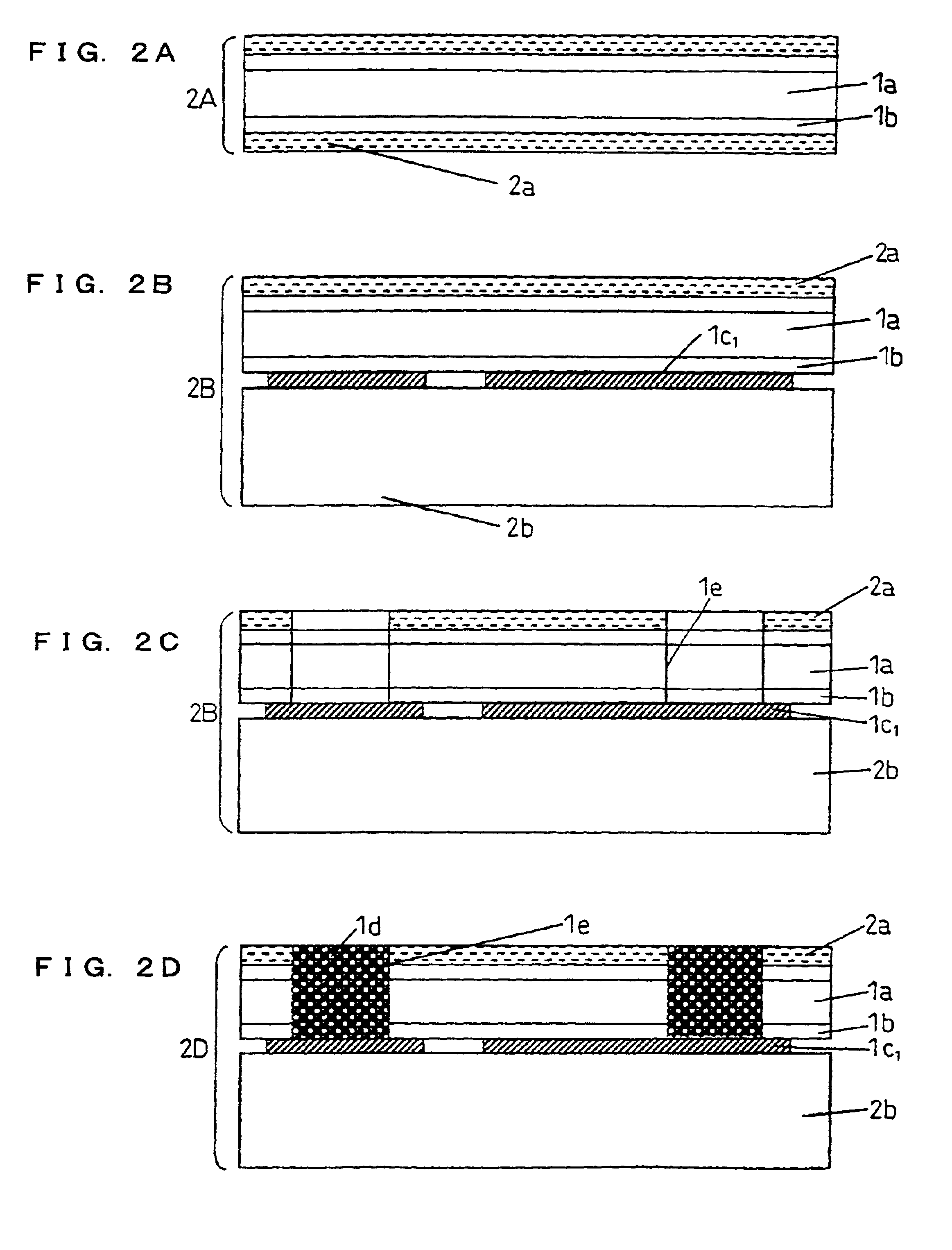
[0078]In this embodiment, upon using a cured product made from a conductive powder and an epoxy resin as the conductive paste 1d, a mixture of an imide series adhesive with an epoxy series adhesive is used as the resin adhesive layer 1b.
[0079]Thus, this embodiment is characterized in that the content of the epoxy series adhesive in the resin adhesive layer 1b is made lower than the content of the epoxy series adhesive in the conductive paste 1d. Here, since the basic construction of this both-sided circuit substrate is similar to the both-sided circuit substrate described with reference to FIGS. 2 and 3, the description thereof will be omitted.
[0080]As a comparative example according to this embodiment, the following is prepared. Namely, upon using a cured product made from a conductive powder and an epoxy resin as the conductive paste 1d, a mixture with an epoxy series adhesive is used as the resin adhesive layer 1b. Further, in the comparative example, the content of the epoxy se...
third embodiment
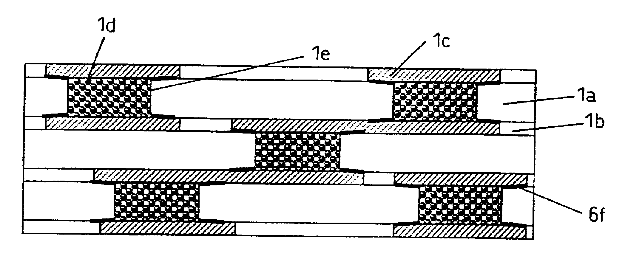
[0083]FIG. 7 is a cross-sectional view showing a multi-layer circuit substrate (made of four layers in FIG. 7) according to third embodiment of the present invention. Here, since the basic construction of this multi-layer circuit substrate is similar to the multi-layer circuit substrate described with reference to FIG. 1, the description thereof will be omitted.
[0084]In this embodiment, in such a multi-layer circuit substrate, the conductive powder 4e constituting the conductive paste 1d and the wiring layer 1c assume the following construction at the contact interface thereof. Namely, a metal cohesion 4f is formed at least at one of the connection points between the conductive powder 4e and the wiring layer 1c.
[0085]When metal cohesion 4f is formed, the bonding strength at the bonding site thereof is enhanced. For this reason, the following relationship is generated when the bonding strength at the bonding site (where metal cohesion 4f is formed) between the wiring layer 1c and th...
PUM
 Abstract
Description
Claims
Application Information
 - Generate Ideas
- Intellectual Property
- Life Sciences
- Materials
- Tech Scout
- Unparalleled Data Quality
- Higher Quality Content
- 60% Fewer Hallucinations
Browse by: Latest US Patents, China's latest patents, Technical Efficacy Thesaurus, Application Domain, Technology Topic, Popular Technical Reports.
© 2025 PatSnap. All rights reserved.Legal|Privacy policy|Modern Slavery Act Transparency Statement|Sitemap|About US| Contact US: help@patsnap.com