Methods for providing a sub .15 micron magnetic memory structure

a magnetic memory structure and sub-.15 micron technology, applied in the field of magnetic systems, can solve the problems of b>60/b> not being able to reliably fabricate smaller magnetic elements, insulators b>60/b> and other features fabricated on the magnetic elements, such as contacts, not being in the appropriate places

Active Publication Date: 2005-08-23
SAMSUNG SEMICON
View PDF4 Cites 264 Cited by
  • Summary
  • Abstract
  • Description
  • Claims
  • Application Information

AI Technical Summary

Benefits of technology

[0012]According to the system and method disclosed herein, the present invention provides a ...

Problems solved by technology

Although the conventional method 10 can be used to fabricate magnetic elements, one of ordinary skill in the art will readily recognize that the use of the conventional method 10 may not reliably fabricate smaller magnetic elements.
However, magnetic elements having a width of less than or equal t...

Method used


Image

  • Methods for providing a sub .15 micron magnetic memory structure
  • Methods for providing a sub .15 micron magnetic memory structure
  • Methods for providing a sub .15 micron magnetic memory structure

Examples


second embodiment

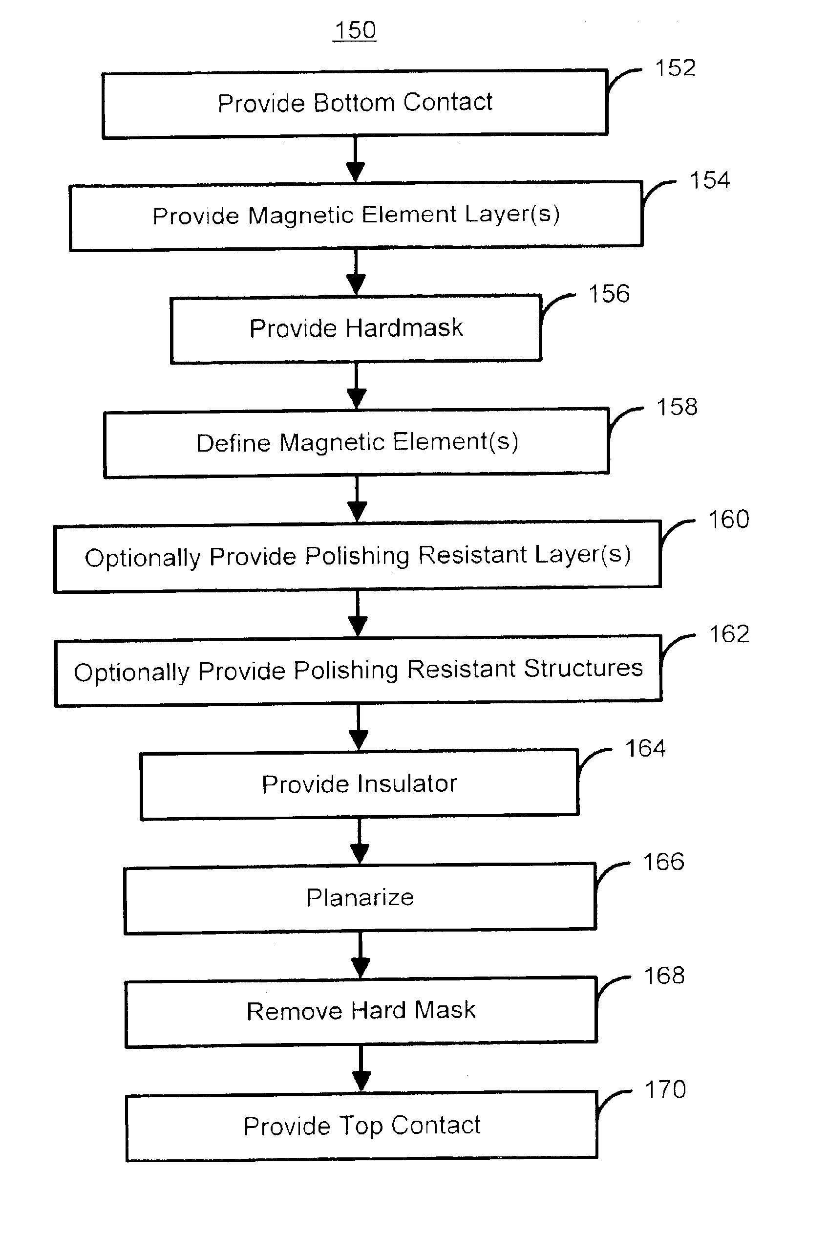
[0056]FIGS. 10A-10G depict system 400 including one embodiment of a magnetic element in accordance with the present invention during fabrication. When completed, the system 400 includes a magnetic element; such as the magnetic elements 70, 80, 90 and 90′; that employs the spin transfer phenomenon in order to switch the direction of magnetization of one or more free layers. FIGS. 10A-10G are described in conjunction with the method 150 depicted in FIG. 8. Referring to FIGS. 8 and 10A-G, FIG. 10A depicts the system 400 after step 152, formation of the bottom contact. The system includes substrate 402 having CMOS circuitry. The bottom contact 404 has been formed between insulators 406 that are preferably SiO2. The bottom contact 404 connects the magnetic element to CMOS based circuitry, which enables one element to be electrically selected from within a dense array. Also depicted are polishing resistant structures 408, such as Si3N4 structures. The Si3N4 structures 408 are thus formed ...

third embodiment

[0060]FIGS. 11A-11C depict system 500 including one embodiment of a magnetic element in accordance with the present invention during fabrication. When completed, the system 500 includes a magnetic element; such as the magnetic elements 70, 80, 90 and 90′; that employs the spin transfer phenomenon to switch the direction of magnetization of one or more free layers. FIGS. 11A-11C are described in conjunction with the method 150 depicted in FIG. 8. Referring to FIGS. 8 and 11A-C. The system 500 does not include Si3N4, or polishing resistant structures. Consequently, the system 500 resembles the system 300 until after the magnetic element is defined in step 158. Thus, 11A depicts the system after the insulator has been deposited in step 164, with step 162 being omitted. The system 500 includes a substrate 502 having CMOS circuitry. The bottom contact 504 has been formed between insulators 506 that are preferably SiO2. The bottom contact 504 connects the magnetic element to CMOS based ci...

fourth embodiment

[0063]FIGS. 12A-12C depict system 600 including one embodiment of a magnetic element in accordance with the present invention during fabrication. When completed, the system 600 includes a magnetic element, such as the magnetic elements 70, 80, 90 and 90′, that employs the spin transfer phenomenon in order to switch the direction of magnetization of one or more free layers. FIGS. 12A-12C are described in conjunction with the method 150 depicted in FIG. 8. Referring to FIGS. 8 and 12A-C. The system 600 does not include polishing resistant structures. Consequently, the system 600 resembles the system 300 until after the magnetic element is defined in step 158. Thus, 12A depicts the system after the insulator has been deposited in step 164, with step 162 being omitted. However, the step 164 that formed the insulator also includes forming a polishing resistant layer.

[0064]Thus, the system 600 includes a substrate 602 having CMOS circuitry. The bottom contact 604 has been formed between i...


PUM


Abstract

A method for providing a magnetic element is disclosed. The method includes providing at least one magnetic element layer and providing a hard mask structure for masking a portion of the at least one magnetic element layer. The hard mask structure is made from hard mask material(s) that are etchable for defining the hard mask structure. The hard mask structure also acts as a mask during definition of a width of the magnetic element. The method also includes defining the width of the magnetic element by removing a portion of the at least one magnetic element layer using the hard mask structure as a mask. The hard mask structure preferably acts as a polishing stop for a planarization step, such as a chemical mechanical polish, polishing resistant structures might be provided to improve planarization of a magnetic memory incorporating the magnetic element.

Description

CROSS-REFERENCE TO RELATED APPLICATIONS[0001]The present application is related to U.S. patent application Ser. No. 10 / 231,430 entitled “Off-Axis Pinned Layer Magnetic Element Using Spin Transfer and an MRAM Device Using the Magnetic Element” filed on Aug. 28, 2002, and assigned to the assignee of the present application. The present application is related to U.S. patent application Ser. No. 10 / 213,537 entitled “Magnetic element utilizing Spin Transfer and an MRAM Device Using the Magnetic Element,” filed on Aug. 6, 2002, and assigned to the assignee of the present application. The present application is related to U.S. patent application Ser. No. 10 / 339,962 entitled “Magnetostatically Coupled Magnetic Elements Utilizing Spin Transfer and an MRAM Device Using the Magnetic Element,” filed on Jan. 10, 2003, and assigned to the assignee of the present application. The present application is related to U.S. patent application Ser. No. 10 / 259,129 entitled “Thermally Stable Magnetic Eleme...

Claims


Application Information

Patent Timeline
IPC IPC(8): H01L21/00H01L43/12
CPCH01L43/12H10N50/01
Inventor ALBERT, FRANKHUAI, YIMINGNGUYEN, PAUL P.
Owner SAMSUNG SEMICON
Why Eureka
Try Eureka