
Test mark and electronic device incorporating the same

a technology of electronic devices and test marks, applied in the direction of identification means, electrical apparatus casings/cabinets/drawers, instruments, etc., can solve the problems of defective connection, difficult to perfectly align the very closely spaced leads with each other, adverse effect of injection current, etc., to improve test accuracy, improve efficiency, and improve inspection efficiency

Inactive Publication Date: 2005-08-30
TOHOKU PIONEER CORP
View PDF3 Cites 21 Cited by
  • Summary
  • Abstract
  • Description
  • Claims
  • Application Information

AI Technical Summary

Benefits of technology

The present invention provides a test mark for checking the quality of interconnections between components in a display panel, such as a panel substrate, TAB tape, and flexible board. The test mark is formed by combining two test marks, which are tested for electrical connection after they are connected together. The test mark can be easily detected using a microscope or a light-emitting device. The invention also provides a method for efficiently inspecting the interconnections and improves the reliability of electronic devices that have components interconnected with high reliability.

Problems solved by technology

However, it is still difficult to perfectly align the very closely spaced leads with each other even through the alignment using the aforementioned alignment marks because of a lack in resolution of the picked-up images or individual errors in the substrate glass, TAB tape, and FPC caused when they are formed.
Additionally, in the pressure pre-attachment or the final pressure attachment process after alignment, dislocation or defective pressure attachment may occur to result in defective connection.
In particular, for a display panel such as an organic EL display panel including current injection display elements, even a slight dislocation may decrease the contact area between the interconnected leads, hence bringing about an adverse effect on the injection current.
The decrease in contact area between the leads (even they are securely connected to each other) can degrade display performance.
However, it is impossible to know thoroughly by the visual inspection whether the contact area is properly left between the leads.
Additionally, the aforementioned alignment marks for alignment are too small to be used for the visual inspection to check for misalignment.

Method used


Image

  • Test mark and electronic device incorporating the same
  • Test mark and electronic device incorporating the same
  • Test mark and electronic device incorporating the same

Examples


Embodiment Construction

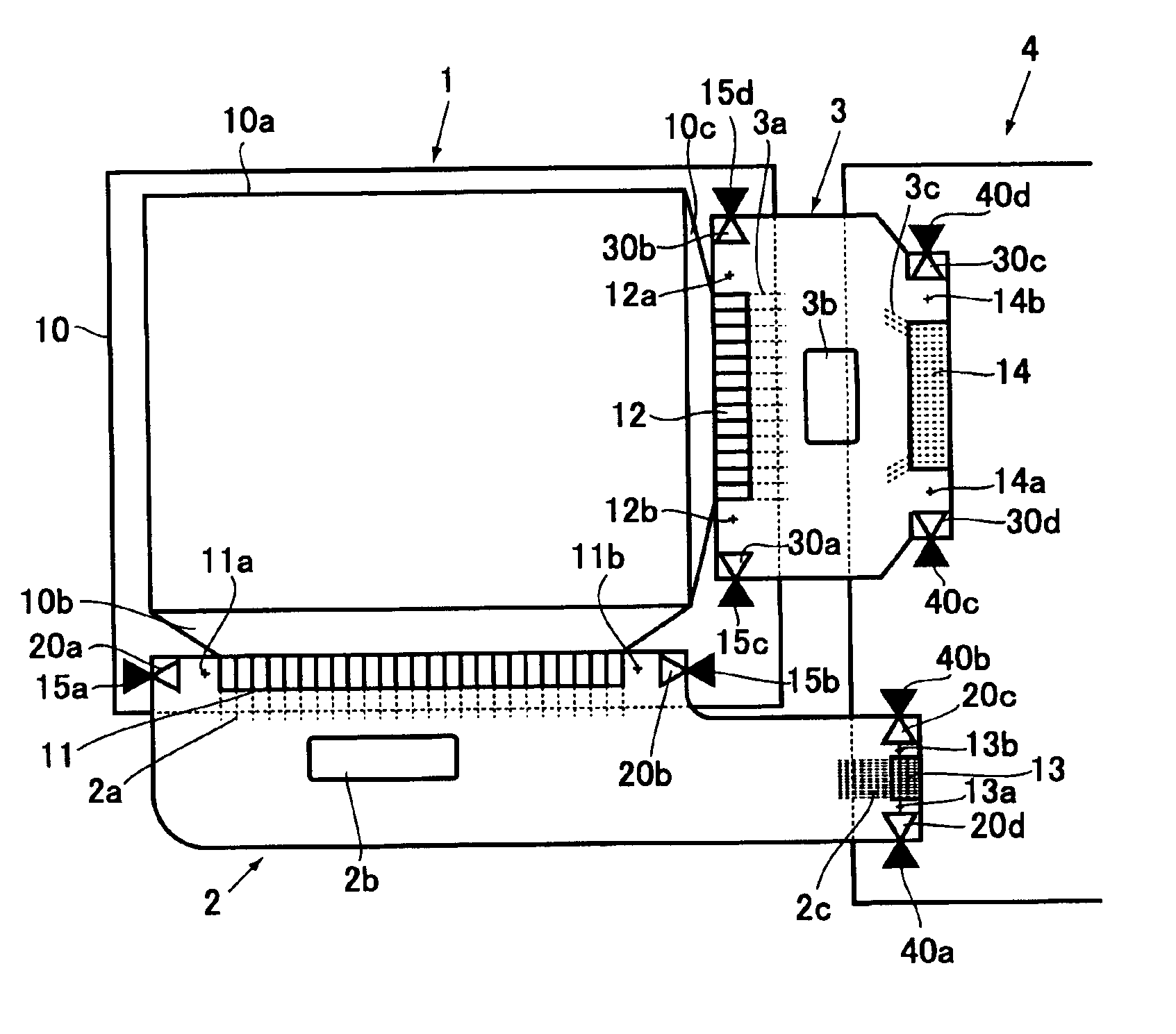
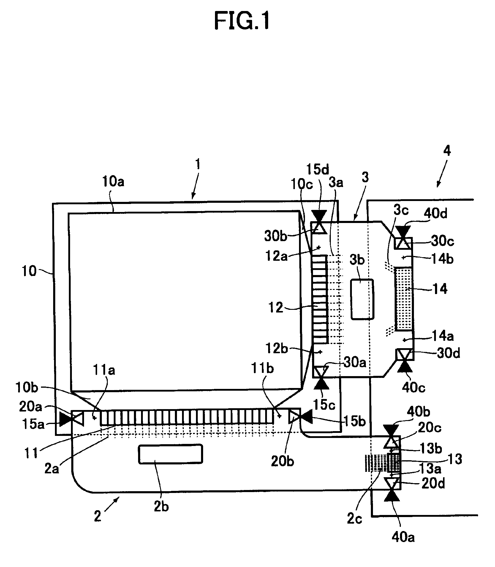
[0040]Now, the present invention will be described below with reference to the accompanying drawings in accordance with the embodiments. FIG. 1 is an explanatory view illustrating an embodiment of the present invention, showing electronic components mounted on a display panel and test marks arranged thereon. As illustrated, there are provided an organic EL display panel 1, TAB tapes 2 and 3, and a flexible board 4.

[0041]A panel substrate 10 of the organic EL display panel 1 has signal lines or leads 10b, 10c extending from a display area 10a, in which the leads 10b and 10c are arranged in a closely spaced relation, respectively, to be connected to leads 2a and 3a of the TAB tapes 2 and 3 at connection areas 11 and 12, respectively. There are also provided ICs 2b and 3b which are bonded on the TAB tapes 2 and 3.

[0042]Leads 2c and 3c of the TAB tapes 2 and 3 on the side of the flexible board 4 are connected to connection lines of the flexible board 4 at connection areas 13 and 14 prov...


PUM

PropertyMeasurementUnit
flexibleaaaaaaaaaa
electrical connectionaaaaaaaaaa
distanceaaaaaaaaaa

Abstract

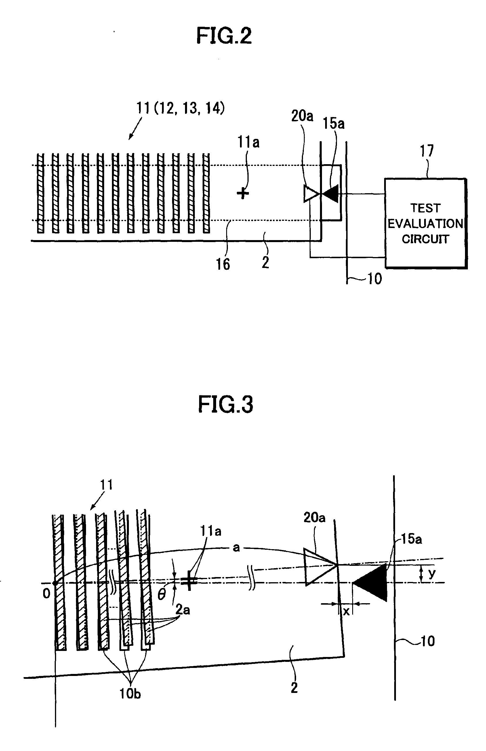
A test mark is provided, for use in an inspection after a display panel, TAB tapes, and a flexible board have been connected together. Defective panels can be rejected with high accuracy in the simple inspection, thereby mitigating the burden on the microscopic inspection. At a predetermined distance from each of connection areas for connecting a panel substrate, TAB tapes, and a flexible board, there are provided test marks with at least one on each component. The electrical connection is tested between each pair of the test marks to thereby determine whether the interconnection is in a good state.

Description

BACKGROUND OF THE INVENTION[0001]The present invention relates to a test mark which is provided on a connection for interconnecting at least two of a panel substrate, TAB tape, and flexible board of a display panel to easily check for any defect in the connection, and also relates to an electronic device with a display panel, a TAB tape, or a flexible board which are provided with this test mark thereon.[0002]The present application claims priority from Japanese Application No. 2002-42558, the disclosure of which is incorporated herein by reference for all purposes.[0003]As portable telephones and portable digital assistants (PDAs) have become widely available, small and thin display panels with a high display capability have been increasingly demanded. Liquid crystal display panels or organic EL (electroluminescent) display panels have been employed as the display panel which meet the demand.[0004]To improve the display capability of such a display panel, it is critical to mount el...

Claims


Application Information

Patent Timeline
Patent Type & Authority Patents(United States)
IPC IPC(8): G01R31/02G01R31/04G09G3/00H05K3/36H05K1/02G02F1/13G02F1/1345G09F9/00H01L21/60H05K1/14
CPCG01R31/04G09G3/006H05K3/361H05K1/0268H05K2201/09781H05K2203/162G01R31/66
Inventor OHAZAMA, HIDETAKA
Owner TOHOKU PIONEER CORP
Learn More