Method for manufacturing a substrate and a display device

a technology of display device and substrate, which is applied in the manufacture of electrode systems, instruments, electric discharge tubes/lamps, etc., can solve the problem of taking a long time to evacuate panel space, and achieve the effect of reducing the size of the manufacturing apparatus, improving the manufacturing rate, and facilitating the electrical process

Inactive Publication Date: 2005-08-30
CANON KK
View PDF8 Cites 3 Cited by
  • Summary
  • Abstract
  • Description
  • Claims
  • Application Information

AI Technical Summary

Benefits of technology

[0014]It is an object of the present invention to provide an apparatus for manufacturing an electron source including a voltage-applying probe, in which the probe has improved electrical connectivity and durability, and wherein a reduction in size and facilitation of operations are enabled. It is another object of the present invention to provide a method for manufacturing an electron source, in which cost, and the amount of work and time for manufacturing can be saved, and manufacturing rate improved, thus enabling the method to be suitable for use in mass production of electron sources. It is another object of the present invention to provide an apparatus for manufacturing an electron source having superior electron-emitting characteristics relative to at least some other electron sources. It is a further object of the present invention to provide a method for manufacturing an electron source using the apparatus.
[0020]As described above, in accordance with the present invention, an apparatus for manufacturing and electron source includes a base for supporting a substrate preliminarily provided with conductors and a container for covering the substrate supported by the base. The container covers the surface of the substrate partially, and thus it is possible to form an airtight space on the substrate with the electrically conductive lines (wirings) connected to the conductors formed on the substrate being partially exposed to the environment outside of the container. The container also is provided with a gas inlet and a gas outlet. The inlet and outlet are connected to a unit for introducing a gas into the container and a unit for discharging a gas from the container, respectively. By virtue of these features, the atmosphere inside the container can be controlled to achieve desired conditions. The substrate preliminarily provided with the conductors is a substrate in which electron-emitting sections are formed in the conductors by a predetermined electrical process to produce an electron source. Therefore, the manufacturing apparatus of the present invention further includes a unit for performing the electrical process, for example, a unit for applying a voltage to the conductors. In such a manufacturing apparatus, a reduction in manufacturing apparatus size is achieved. Moreover, operations, such as making an electrical connection to a power source during the electrical process, can be facilitated by the voltage-applying probe as described above, and further there is freedom provided with regard to the design for the size and shape of the container so that introduction of the gas into the container and discharge of the gas from the container can be performed quickly.
[0021]In another aspect of the present invention, in a method for manufacturing an electron source, a substrate on which conductors and electrically conductive lines (wirings) connected to the conductors are preliminarily formed is placed on a base, and the conductors on the substrate are covered by a container, although parts of the lines preferably are not so covered. Thus, the conductors are placed in an airtight space formed with the substrate and the container, and the lines formed on the substrate are partially exposed to the environment outside of the container. Next, the atmosphere in the container is controlled to achieve desired conditions, and a predetermined electrical process is performed on the conductors via the parts of the lines exposed to the outside of the container; for example, a voltage is applied to the conductors. The desired atmosphere is, for example, a reduced-pressure atmosphere or an atmosphere in which a predetermined gas is present. The electrical process is a process in which electron-emitting portions are formed in the conductors to produce an electron source (electron-emitting device). The electrical process may be performed a plurality of times in different atmospheres. For example, after the conductors on the substrate are covered by the container, excluding covering parts of the lines, the electrical process is performed in a first atmosphere, and then the electrical process is performed again in a second atmosphere. Desired electron-emitting portions are thereby formed in the conductors and an electron source is produced. Preferably, the first atmosphere is a reduced-pressure atmosphere, and the second atmosphere is an atmosphere in which a gas composed of a carbon compound or the like is present. In the present manufacturing method, electrical connection to a power source, etc., in the electrical process may be facilitated by the use of the voltage-applying probe described above. Since, as described above, there is freedom with regard to the design for the size and shape of the container, etc., introduction of a gas into the container and discharge of a gas from the container can be performed quickly, thereby improving the manufacturing rate as well as improving consistency in the electron emission characteristics of the electron sources manufactured. In particular, uniformity is provided in the electron-emitting characteristics of a manufactured electron source having a plurality of electron-emitting portions. Consequently, in accordance with an aspect of the present invention, it is possible to provide an image-forming apparatus capable of producing images having superior quality relative to those produced by prior art apparatuses.

Problems solved by technology

In the second manufacturing method, it takes a long time to evacuate the panel space and to introduce the gas containing the organic substance into the panel space.

Method used


Image

  • Method for manufacturing a substrate and a display device
  • Method for manufacturing a substrate and a display device
  • Method for manufacturing a substrate and a display device

Examples


example 1

[0069]In this example, an electron source provided with a plurality of surface-conduction electron-emitting devices was manufactured using a manufacturing apparatus in accordance with the present invention.

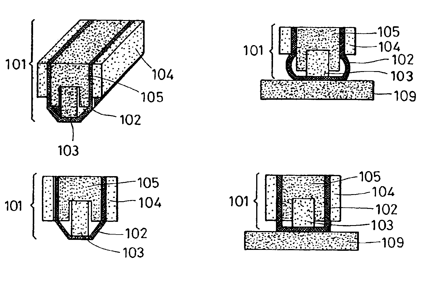
[0070]In a mesh sheet 115 shown in FIG. 7, a plurality of linear members 106A and 106B composed of a resin were woven into a mesh. The linear members 106A and 106B may be composed of, for example, a metal. In FIG. 8, as a conductive sheet 102, a mesh circuit connector (MCC), such as that manufactured by NBC Inc., was used, in which a conductive material layer 108 composed of copper or the like was formed (deposited) on the mesh sheet 115 (FIG. 7). The conductive material layer 108 may be composed of aluminum or gold. Alternatively, the conductive material layer 108 may have a multi-layered structure formed of copper-nickel-gold. In order to form the conductive material layer 108, plating was used. FIG. 9 is a cross-sectional view of the conductive sheet 102 in which the conductive...

example 2

[0076]In this example, a probe 101 was used which had substantially the same structure as that of the probe used in Example 1, apart from the fact that the lower parts of the sides of the block 105 were not covered by the support plates 104, as shown in FIG. 11. FIG. 12 is a cross-sectional view showing a state in which the probe 101 was pressed against the lines (not shown in FIG. 12) on a substrate 109. As shown in FIG. 12, the conductive sheet 102 became deformed so as to protrude at an area below the sides of the block 105. Due to such a deformation, the probe 101 was pressed against the lines on the substrate 109 without bending at the area of the conductive sheet 102 in contact with the lines, and without a locally applied load. Even if the probe 101 was used repeatedly, the conductive material layer 108 (FIG. 8) formed on the conductive sheet 102 was not disconnected or detached, and thereby durability was improved. In this example, the same advantages as those of Example 1 w...

example 3

[0078]In a probe 101 shown in FIG. 15, an elastic member 103 was fixed to a support plate 114 by an elastic fixing plate 110 and an elastic bar 111, and a conductive sheet 102 was fixed on blocks 105 at the sections supported by support plates 104. The blocks 105 were fixed on a block holding plate 112. By connecting the block holding plate 112 to the support plate 114 via a spring 113, the elastic member 103 was supported separately from the blocks 105 for supporting the conductive sheet 102 so as to be independently movable. In another embodiment, an elastic material, such as rubber, may be used instead of the spring 113.

[0079]When the probe 101 having the structure described above was pressed against at least one line formed on a substrate (not shown in FIG. 15), although the elastic member 103 shrank, since the conductive sheet 102 was not deformed, the probe 101 was pressed against the line without bending of the conductive sheet 102 in the area pressed against line and without...


PUM

PropertyMeasurementUnit
angleaaaaaaaaaa
widthaaaaaaaaaa
pressureaaaaaaaaaa

Abstract

A probe for applying a voltage to lines provided on a substrate comprises (a) a conductive sheet, the conductive sheet including a mesh sheet in which linear members are woven into a mesh and a conductive material which coats the mesh sheet, (b) an elastic member for pressing the conductive sheet against the lines, and (c) a holding member for holding the conductive sheet and the elastic member together. The probe has improved electrical connectivity and durability, and achieves a reduction in size and facilitation of operations of an apparatus for manufacturing an electron source.

Description

[0001]This application is a division of U.S. application Ser. No. 10 / 143,783, filed May 14, 2002, now U.S. Pat. No. 6,741,087.BACKGROUND OF THE INVENTION[0002]1. Field of the Invention[0003]The present invention relates to a probe used for applying a voltage, and to an apparatus for manufacturing an electron source, the apparatus including the probe.[0004]2. Description of the Related Art[0005]Electron-emitting devices included in electron sources are generally classified as being one of two types: thermionic cathode and cold cathode. Examples of cold cathode include field-emission type electron-emitting devices, metal / insulating layer / metal type electron-emitting devices, and surface-conduction type electron-emitting devices.[0006]The operation of a surface-conduction type electron-emitting device is based on a phenomenon wherein electron emission occurs when a current is passed through a thin, small film formed on a substrate, in parallel with the film surface. The basic structure...

Claims


Application Information

Patent Timeline
Patent Type & Authority Patents(United States)
IPC IPC(8): H01J9/02G01R1/06
CPCH01J9/02Y10T29/49204H01J2329/00H01J2201/3165
Inventor KIMURA, AKIHIROOKI, KAZUHIROKAMATA, SHIGETO
Owner CANON KK
Why Eureka
Try Eureka