Method for testing an integrated circuit with an external potential applied to a signal output pin

a technology of external potential and signal output pin, which is applied in the direction of individual semiconductor device testing, measurement instrument housing, instruments, etc., to achieve the effect of preventing crosstalk between adjacent windows of discriminators, simple and inexpensive manner, and easy separation

Inactive Publication Date: 2005-08-30
ATMEL GERMANY +2
View PDF19 Cites 5 Cited by
  • Summary
  • Abstract
  • Description
  • Claims
  • Application Information

AI Technical Summary

Benefits of technology

[0013]In a development of the method, it is advantageous to test the values of the potential values applied at the signal output for conformity with a reference value by means of a control unit during a defined time window before switching the integrated circuit into the test mode, and to switch the integrated circuit into the test mode in a second time window provided that the potential value available at the signal output corresponds to the defined reference value. In so doing, it is advantageous if the potential value set at the signal output remains constant over time and the test signal represents an alternating voltage. The direct voltage components can thus be easily separated with an external measurement arrangement. In comparison to the previous state of the art, an integrated circuit can be switched into a test mode by means of a single resistor in a particularly simple and inexpensive manner with the method according to the invention.
[0014]In the case of a plurality of signal outputs, it is possible in a development of the method for the control unit to test the potential value set at a first signal output and apply the test signal at another, e.g. second, signal output. The advantages of this are that there is no superimposition with the set direct voltage value and that a direct voltage offset of the test signal can be measured.
[0015]In another development of the method, the control unit performs a Boolean logic operation with the potential value set at the signal output and a signal of a circuit component of the circuit unit. An AND logic operation with the negative signal value enables, for example, the integrated circuit to be prevented from being switched into a test mode by a potential available at the signal output. For this purpose, it is advantageous if the logic operation is performed with a control voltage from an output stage of the integrated circuit. This embodiment of the method according to the invention enables the test signal in the test mode to be prevented from being superimposed at the signal output on the output signals available in normal operation, that is if input signals are available for example, in a particularly reliable manner.
[0016]Investigations by the applicant have shown that it is advantageous if different test signals are selected as a function of the voltage values set at the signal output, in that, for example, specific parts of the circuit are activated or deactivated by the control unit when there are defined potential values within the circuit unit. In this manner, defined signal shapes can be generated in the case of the test signals with or without an available input signal.
[0017]In a further development of the method according to the invention, the integrated circuit is switched into the test mode if the potential value available at the signal output of the integrated circuit lies within a voltage interval of a voltage window discriminator. In so doing, it is advantageous if the signal heights of the test signals, that is their amplitudes and their direct voltage offsets, are set by means of signal amplifiers so that the direct voltage offset of the respective test signal corresponds to the potential value Bet at the signal output, and the maximum amplitude of the test signal lies within the interval defined by the respective window of the discriminator. Crosstalk between adjacent windows of the discriminators can be prevented in this way provided that a plurality of window discriminators are used. Furthermore, the direct voltage value at the signal output is little changed.
[0018]The present, new circuit arrangement can be used in an advantageous manner for implementing the method according to the invention. An advantage of the integration of a control unit and at least one switching element according to the second-mentioned object of the present invention is that all internal measuring pads may be eliminated while incurring little additional circuit complexity. Another advantage is that a single resistor, which is connected externally to the signal output, is sufficient to switch the integrated circuit into a test mode if the supply voltage is available.

Problems solved by technology

Moreover, it is irrelevant to the new method whether or not an input signal is available at a signal input of the integrated circuit.

Method used


Image

  • Method for testing an integrated circuit with an external potential applied to a signal output pin
  • Method for testing an integrated circuit with an external potential applied to a signal output pin
  • Method for testing an integrated circuit with an external potential applied to a signal output pin

Examples


Embodiment Construction

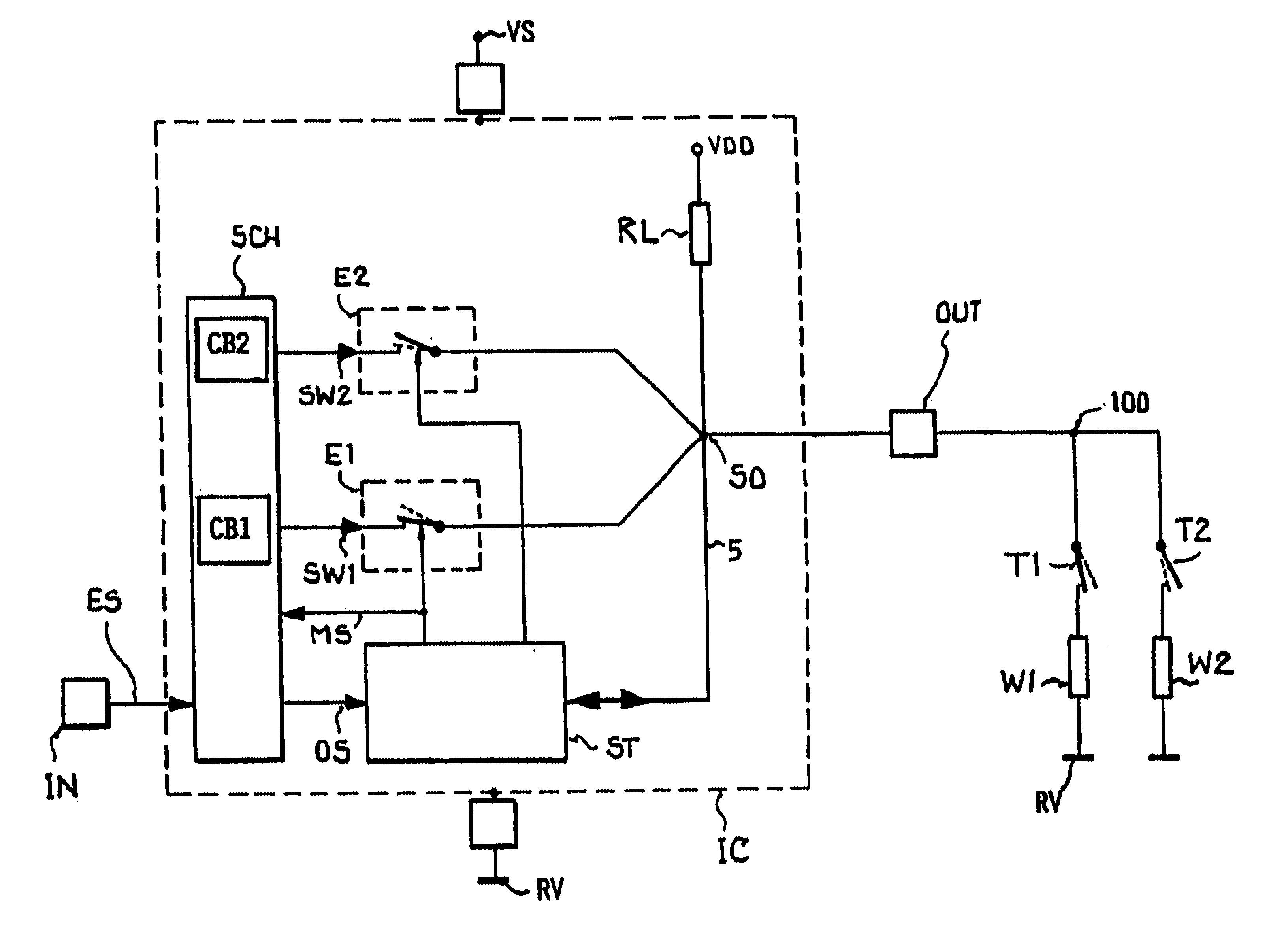
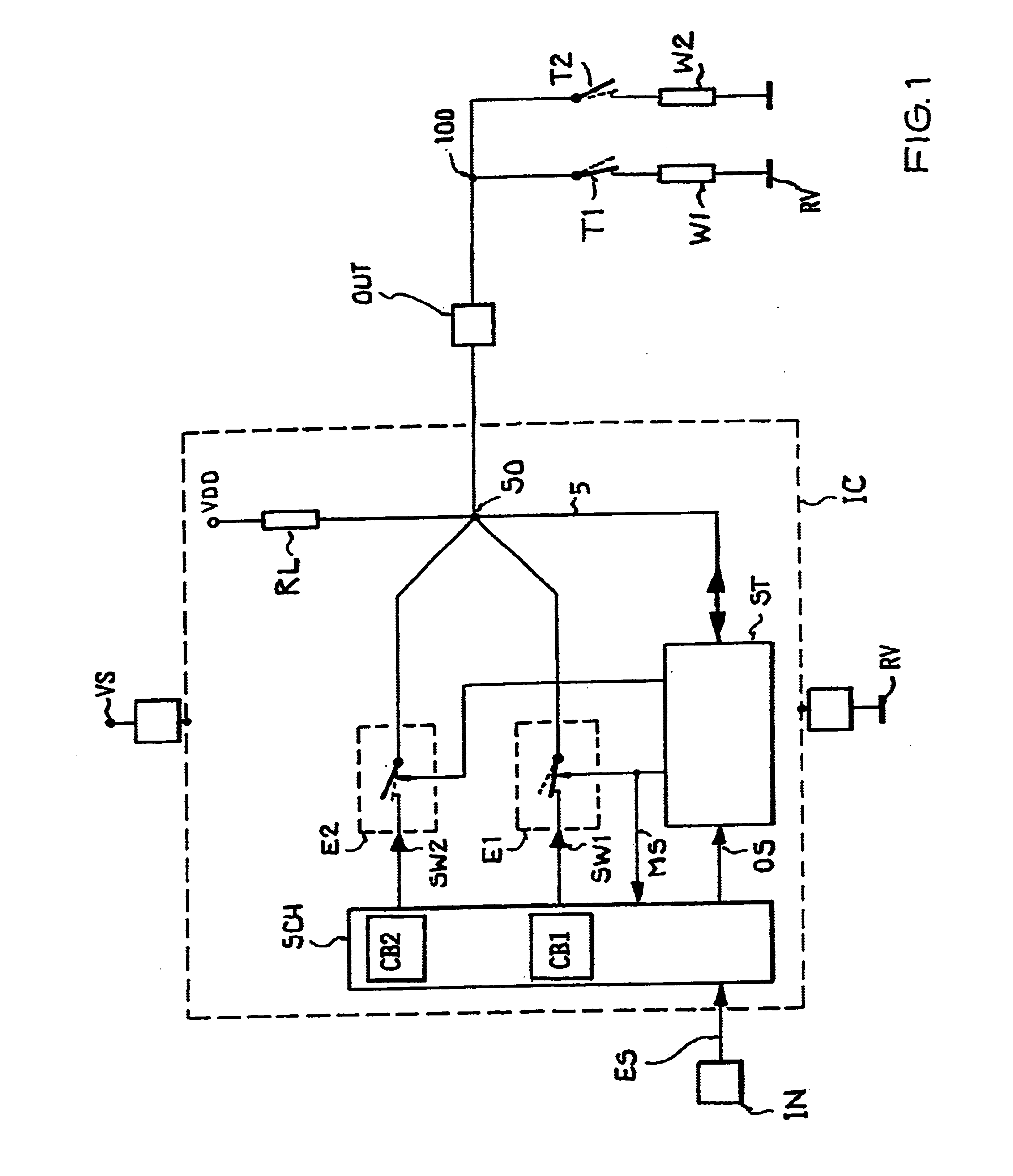
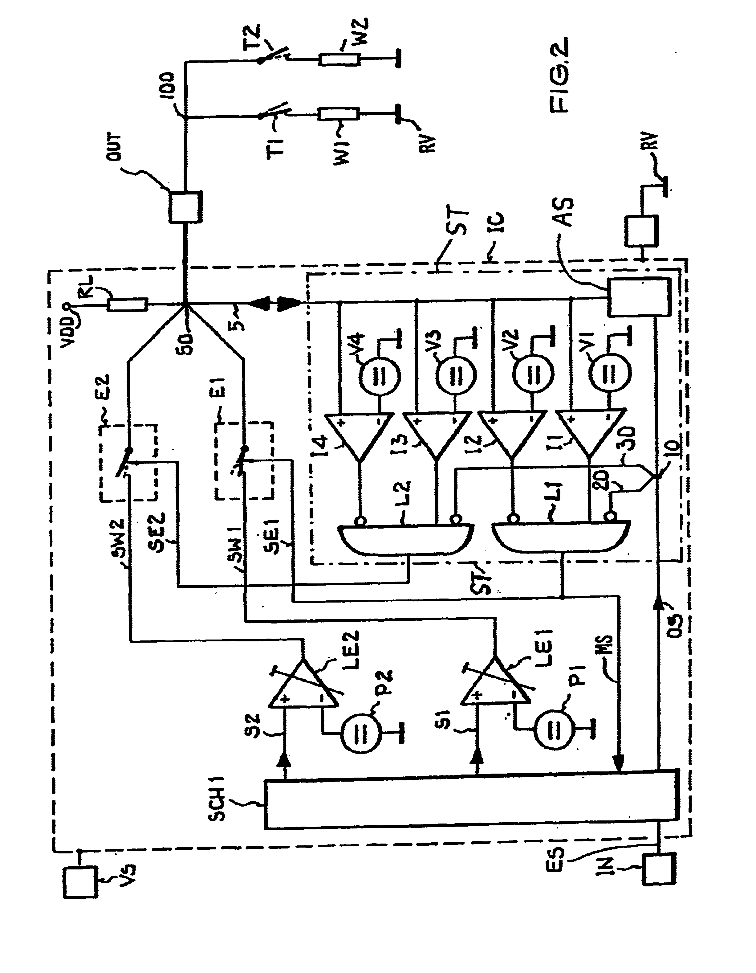
[0023]The object of the integrated circuit IC shown in FIG. 1 is to apply the output signals from a circuit unit as test signals to a signal output of the integrated circuit provided that, at the signal output, an externally applied potential value, which can be set by means of an external resistor for example, corresponds to a defined reference value. The integrated circuit IC has an input pin IN and an output pin OUT for this purpose. The output pin OUT is externally linked to a reference potential RV via a node 100 which is connected to a resistor W1 by means of a switch T1 or to a resistor W2 by means of a switch T2. Furthermore, the integrated circuit has another pin at which a supply voltage VS is available and a pin which is linked to the reference potential RV.

[0024]There are two functional units within the integrated circuit IC. The first functional unit contains the circuit functions needed for normal operation of the integrated circuit, which are represented, with the exc...


PUM


Abstract

In previously known methods for testing internal signals of an integrated circuit, additional output pins were required which, in general, were linked to additional measuring pads within the integrated circuit.
In the new method, the circuit functions are tested by using the output pins at which the output signal is present during normal operation of the integrated circuit. By means of a simple, external connection, with which a defined voltage value is set at the signal output, the integrated circuit is switched by means of an integrated control unit into a test mode in which it applies selected signals, which are to be tested, at the signal output. There is no need for additional internal measuring pads or additional output pins.

Description

BACKGROUND[0001]1. Field of the Invention[0002]The present invention relates to a method for testing an integrated circuit and a circuit arrangement for performing this method.[0003]2. Description of the Related Technology[0004]In the case of integrated circuits (ICs), electrical measurements are made after the manufacturing process in order to test the circuits. The high degree of complexity makes it necessary to measure not only the output signals of the entire circuit but also the signals of individual internal functional groups of a circuit. In the development phase, additional internal contact surfaces, so-called measuring pads which are assigned to the individual circuit blocks, are integrated for this purpose. Function checks can be performed at these measuring pads provided that the integrated circuits are not yet enclosed in a casing. In the case of the finished integrated circuits, some of the measuring pads are linked to external bond pads for the purpose of checking the ...

Claims


Application Information

Patent Timeline
Patent Type & Authority Patents(United States)
IPC IPC(8): G11C29/04G11C29/48G11C29/46G01R31/3185G01R31/28H01L21/822H01L27/04
CPCG11C29/46G11C29/48G01R31/28
Inventor EICHIN, MATTHIASKURZ, ALEXANDER
Owner ATMEL GERMANY
Why Eureka
Try Eureka