Adaptive programming technique for a re-writable conductive memory device

a memory device and adaptive programming technology, applied in the field of memory devices, can solve the problems of limiting the total size and applications of the memory, requiring a complex refresh algorithm, and non-volatile memory such as flash memory are slower to program, so as to reduce the effect of increasing the resistance of the selected cell

Active Publication Date: 2005-09-06
UNITY SEMICON
View PDF20 Cites 100 Cited by
  • Summary
  • Abstract
  • Description
  • Claims
  • Application Information

AI Technical Summary

Benefits of technology

[0021]It yet another aspect of the invention, a program circuit for a programming a selected cell to a desired resistive state receives a reference level and a selected cell level. The program circuit includes a comparator, a first driver, and a second driver. The first driver can provide a voltage capable of increasing the resistance of the selected cell and the second driver can provide a voltage capable of decreasing the resistance of the selected cell. Which of the drivers is activated is dependent upon the comparator output and the desired resistive state.

Problems solved by technology

Although SRAM, with very fast access times, is the memory of choice for computer applications, its volatility, large size and stand-by current limit the total size and applications of the memory.
Non-volatile memories such as Flash memory are slower to program, and in some cases must erase a large block of memory before being reprogrammed.
DRAM has the smallest cell size, but necessitates a complex refresh algorithm, and is volatile.
For new applications, away from PC applications and into portable applications such as cell phones, personal digital assistants (PDA), digital cameras, camcorders, removable “key-chain” or “USB” disks, the key issues are nonvolatility and low power consumption.
Both types of memory can be relatively fast or relatively slow.
The ROMs that are capable of modifying their data typically require long write cycles that erase entire blocks of data prior to new data being written.
The layout of such devices are not ideal, usually requiring feature sizes of at least 8f2 for each memory cell, where f is the minimum feature size.
However, mere recognition that a two terminal memory element is theoretically capable of being placed in a cross point array does not solve many of the non-trivial problems associated with actually using such a device.
If the data does not verify properly after a pre-determined number of retries, the memory issues a fail diagnostic.
The problem with the above approach is that it is slow, as the memory circuit has to switch back and forth numerous times between read and write modes.

Method used


Image

  • Adaptive programming technique for a re-writable conductive memory device
  • Adaptive programming technique for a re-writable conductive memory device
  • Adaptive programming technique for a re-writable conductive memory device

Examples


Embodiment Construction

[0040]In the following detailed description of the present invention, numerous specific details are set forth in order to provide a thorough understanding of the present invention. However, it will become obvious to those skilled in the art that the present invention may be practiced without these specific details. In other instances, well-known methods, procedures, materials, components and circuitry have not been described in detail to avoid unnecessary obscuring aspects of the present invention. The detailed description is presented largely in terms of simplified semiconductor device terminal I-V characteristics, circuit block diagrams, circuit schematics and timing diagrams. These descriptions and representations are the means used by those experienced or skilled in the art to concisely and most effectively convey the substance of their work to others skilled in the art.

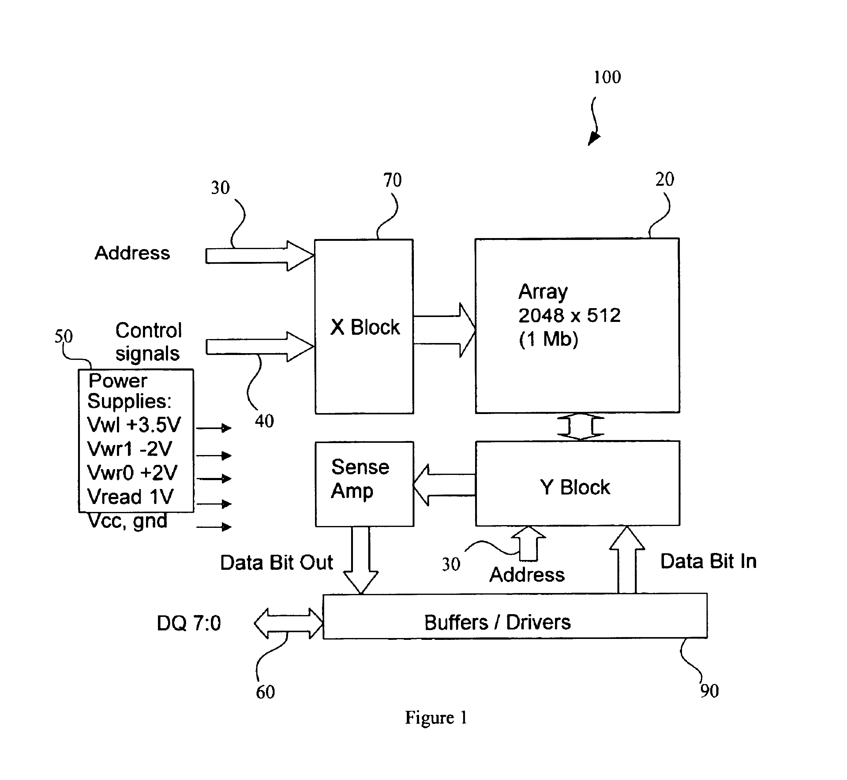
[0041]FIG. 1 depicts one implementation of a block diagram of a memory system 100. The memory system 100, typi...


PUM


Abstract

A programming circuit is provided. As a conductive memory cell is programmed, its resistance changes. The provided programming circuit monitors the changing resistance while programming the memory cell. The programming circuit can be used to only program the memory cell for as long as programming is actually needed. Additionally, the programming circuit can be used to only program the memory cell when it has a value that needs to be changed.

Description

CROSS REFERENCE TO RELATED APPLICATION[0001]This application claims the benefit of U.S. Provisional Application No. 60 / 422,922, filed Oct. 31, 2002, and the U.S. Provisional Application No. 60 / 424,083, filed Nov. 5, 2002, all of which are incorporated herein by reference in their entireties and for all purposes. This application is related to the following U.S. Patent Applications: U.S. application Ser. No. 10 / 360,005, filed Feb. 7, 2003; U.S. application Ser. No. 10 / 330,512, filed Dec. 26, 2002; application Ser. No. 10 / 330,153, filed Dec. 26, 2002; application Ser. No. 10 / 330,964, filed Dec. 26, 2002; application Ser. No. 10 / 330,170, filed Dec. 26, 2002; application Ser. No. 10 / 330,900, filed Dec. 26, 2002; application Ser. No. 10 / 330,150, filed Dec. 26, 2002; application Ser. No. 10 / 330,965, filed Dec. 26, 2002; application Ser. No. 10 / 249,846, filed May 12, 2003; application Ser. No. 10 / 249,848, filed May 12, 2003; application Ser. No. 10 / 612,733, filed Jul. 1, 2003; application ...

Claims


Application Information

Patent Timeline
Patent Type & Authority Patents(United States)
IPC IPC(8): G11C13/00G11C16/02G11C16/10G11C16/34
CPCG11C13/0007G11C13/0064G11C13/0069G11C16/3468G11C2213/31G11C2013/0066
Inventor RINERSON, DARRELLCHEVALLIER, CHRISTOPHE J.
Owner UNITY SEMICON
Why Eureka
Try Eureka