Electromagnetic wave absorber molding material, electromagnetic wave absorber molded element and method of manufacturing same, and electromagnetic wave absorber

a technology of electromagnetic waves and molding materials, which is applied in the direction of shielding materials, thin material processing, and anechoic chambers. it can solve the problems of complex structure, a number of steps to manufacture, and the composite wave absorber type does not exhibit excellent non-flammability. it can achieve the effect of small-sized wave absorbers and non-flammability manufacturing

Inactive Publication Date: 2005-09-13
TDK CORPARATION
View PDF8 Cites 16 Cited by
  • Summary
  • Abstract
  • Description
  • Claims
  • Application Information

AI Technical Summary

Benefits of technology

[0016]It is an object of the invention to provide an electromagnetic wave absorber molding material, an electromagnetic wave absorber molded element and a method of manufacturing the same, and an electromagnetic wave absorber that achieves the manufacture of non-flammable and small-sized wave absorber with ease.

Problems solved by technology

Therefore, the problem is that it is not preferred in some cases to place this wave absorber in a limited space such as a small acechoic chamber, in particular.
Therefore, this type of composite wave absorber does not exhibit excellent non-flammability and it is not suitable for use in the anechoic chamber for safety reasons.
However, the wave absorbing structure using the non-flammable wave absorbing sheet has a problem that the manufacture of the structure requires a number of steps.

Method used


Image

  • Electromagnetic wave absorber molding material, electromagnetic wave absorber molded element and method of manufacturing same, and electromagnetic wave absorber
  • Electromagnetic wave absorber molding material, electromagnetic wave absorber molded element and method of manufacturing same, and electromagnetic wave absorber
  • Electromagnetic wave absorber molding material, electromagnetic wave absorber molded element and method of manufacturing same, and electromagnetic wave absorber

Examples


Embodiment Construction

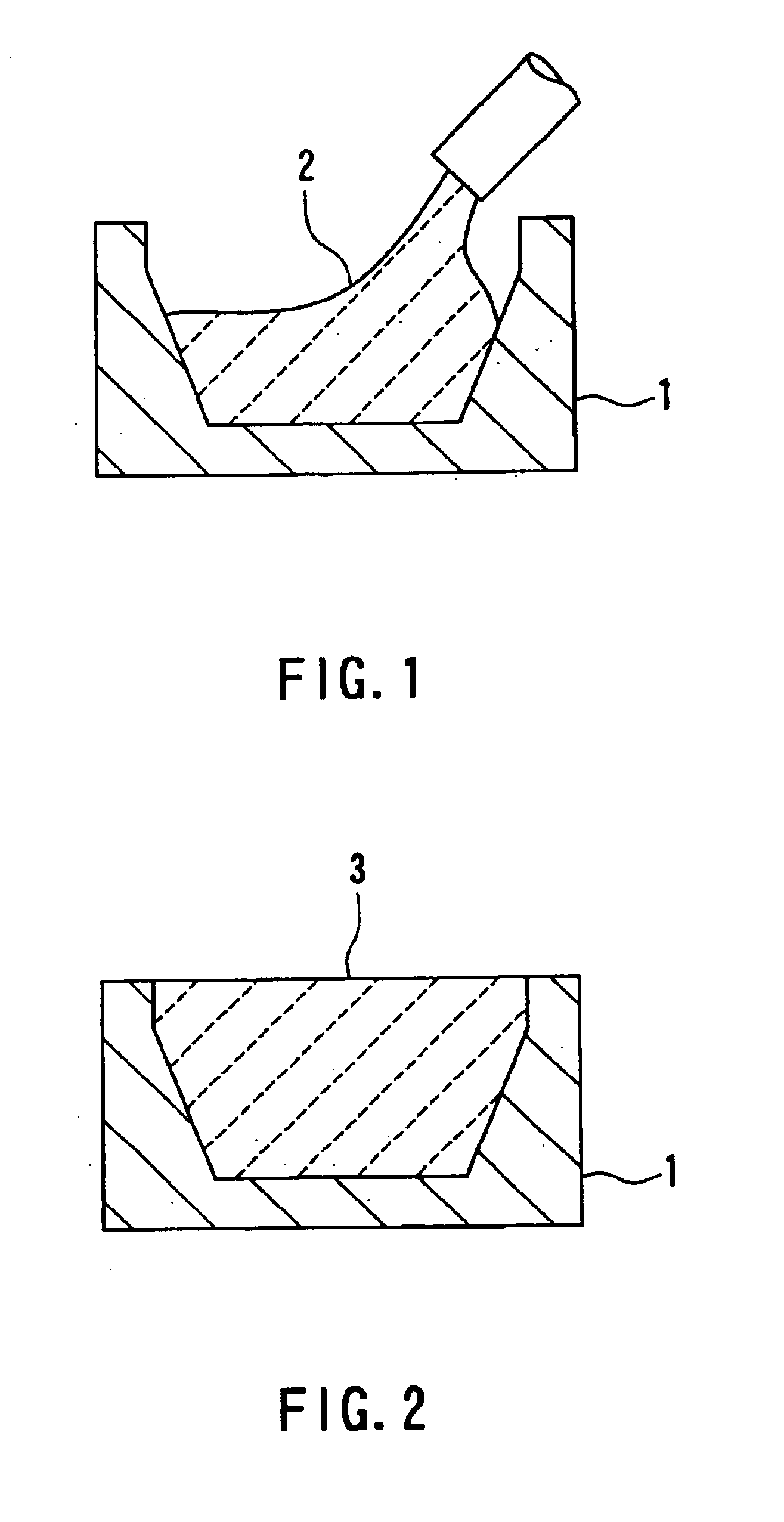
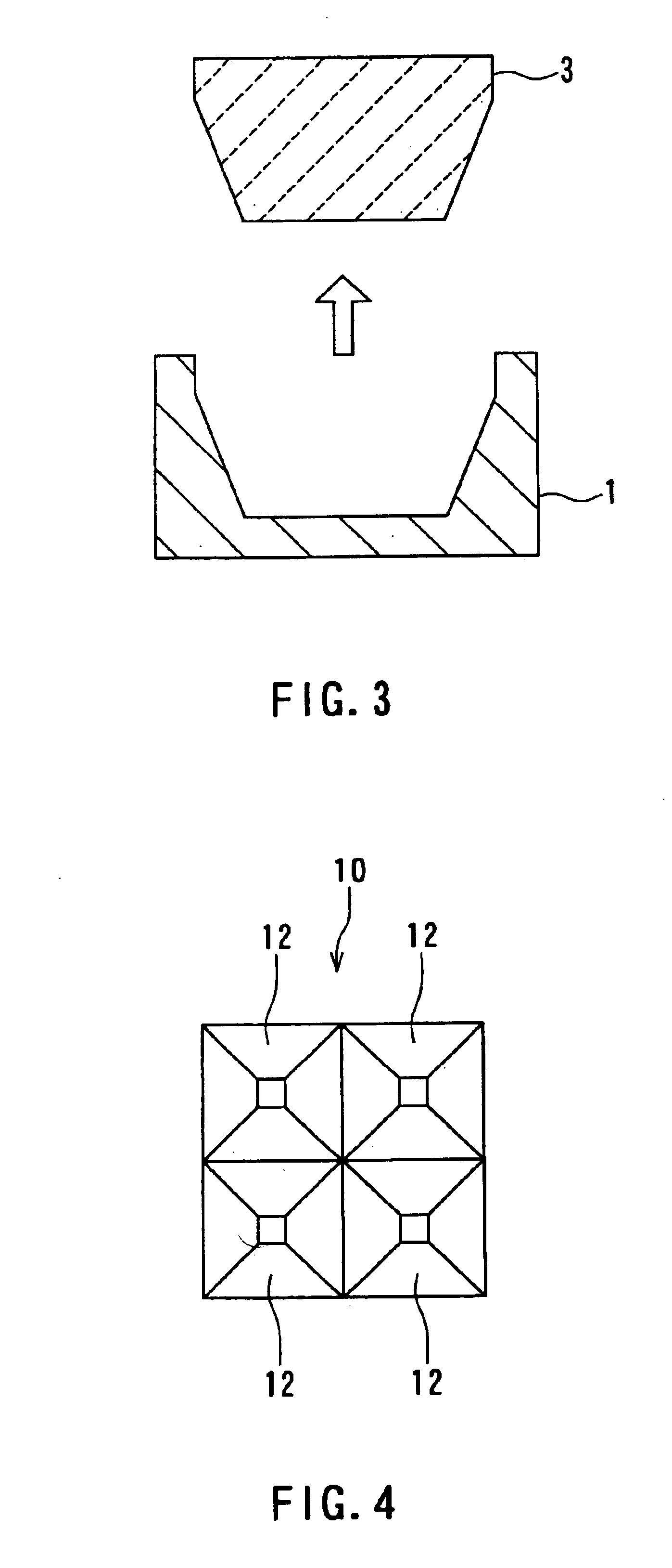
[0038]A preferred embodiment of the invention will now be described in detail with reference to the accompanying drawings.

[Electromagnetic Wave Absorber Molding Material]

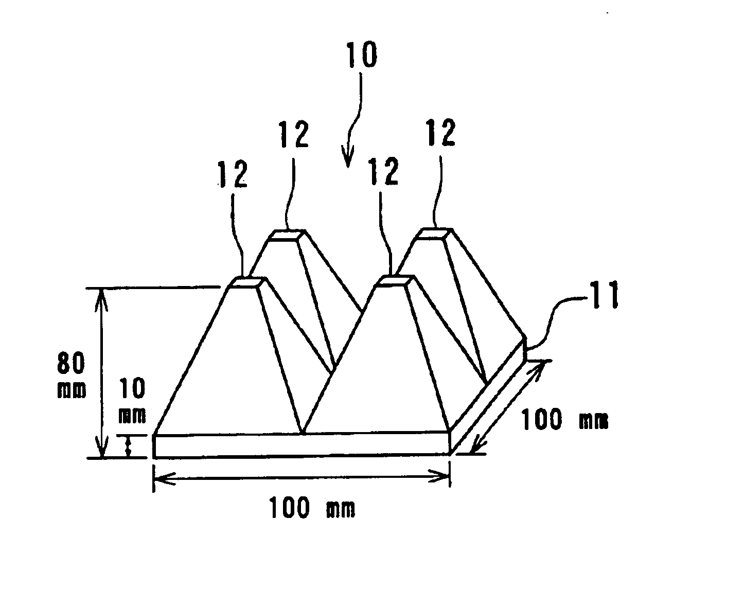
[0039]An electromagnetic wave absorber molding material of an embodiment of the invention will now be described. The material is used for making a molded element making up at least part of an electromagnetic wave absorber. The material includes a magnetic material, inorganic fibers and an inorganic binder. When these ingredients are mixed with water, the molding material first exhibits fluidity and then a curing reaction in a temperature range of 1 to 40° C. inclusive.

[0040]The magnetic material utilized may be ferrite powder, for example. The proportion of the magnetic material in the wave absorber molding material preferably falls within a range of 80 to 90 weight % inclusive.

[0041]The inorganic fibers are fibers made of an inorganic material. Such an inorganic material may be rock wool, glass fibers, silica fiber...


PUM

PropertyMeasurementUnit
temperatureaaaaaaaaaa
lengthaaaaaaaaaa
weight %aaaaaaaaaa

Abstract

An electromagnetic wave absorber comprises an electromagnetic wave absorber molded element, plate-shaped sintered ferrite, and a metal plate. The molded element incorporates a tile-shaped base portion and a wedge-shaped apex portion disposed on the base portion. The molded element is formed by injecting slurry into a mold, the slurry being obtained through mixing a molding material for the wave absorber with water, and curing the slurry. The molding material includes a magnetic material, an inorganic fiber and an inorganic binder. When these ingredients are mixed with water, the molding material first exhibits fluidity and then a curing reaction in a temperature range of 1 to 40° C.

Description

BACKGROUND OF THE INVENTION[0001]1. Field of the Invention[0002]The present invention relates to an electromagnetic wave absorber molding material used for forming a molded element making up at least part of an electromagnetic wave absorber, a wave absorber molded element made of the molding material and a method of manufacturing the molded element, and to the electromagnetic wave absorber including the molded element.[0003]2. Description of the Related Art[0004]It has been commonly practiced to test electromagnetic compatibility (EMC) of a variety of types of instruments in anechoic chambers. The standards concerning EMC define permissible levels and testing methods to comply with for electromagnetic waves generated by the instruments. International standard organizations that establish the standards relating to the EMC include the TC77 and the CISPR that belong to the International Electrotechnical Commission (IEC). These organizations have made basic standards and common standard...

Claims


Application Information

Patent Timeline
Patent Type & Authority Patents(United States)
IPC IPC(8): H05K9/00
CPCH05K9/0075H01Q17/008H01Q17/004Y10T428/25
Inventor KURIHARA, HIROSHIYANAGAWA, MOTONARIHAYASHI, KOZOFUJIMOTO, KYOICHIKISHINO, HIDEKI
Owner TDK CORPARATION
Why Eureka
Try Eureka