Thin film transistor array substrate for a liquid crystal display having repair lines

a thin film transistor and array substrate technology, applied in the field of thin film transistor array substrates for liquid crystal displays, can solve the problems of increased production costs and larger device sizes

Inactive Publication Date: 2005-09-13
SAMSUNG DISPLAY CO LTD
View PDF9 Cites 24 Cited by
  • Summary
  • Abstract
  • Description
  • Claims
  • Application Information

AI Technical Summary

Benefits of technology

[0013]It is an object of the present invention to provide a TFT array substrate for a liquid crystal display that can be fabricated in a cost-effective manner.

Problems solved by technology

First, in the usual TCPs, it is difficult to form as many pads as the number of repair lines. Furthermore, as the number of pads increases, the length of the TCPs for the gate driving IC should increase to be connected to the underlying repair lines. Consequently, TCPs having a special structure would be required, resulting in increased production cost. In addition, either as many interconnection lines for the repair lines should be formed at the PCB as the number of driving ICs, or twice as many. Therefore, the volume of the PCB would be increased, resulting in a larger device size.

Method used


Image

  • Thin film transistor array substrate for a liquid crystal display having repair lines
  • Thin film transistor array substrate for a liquid crystal display having repair lines
  • Thin film transistor array substrate for a liquid crystal display having repair lines

Examples


Embodiment Construction

[0024]Preferred embodiments of this invention will be explained with reference to the accompanying drawings.

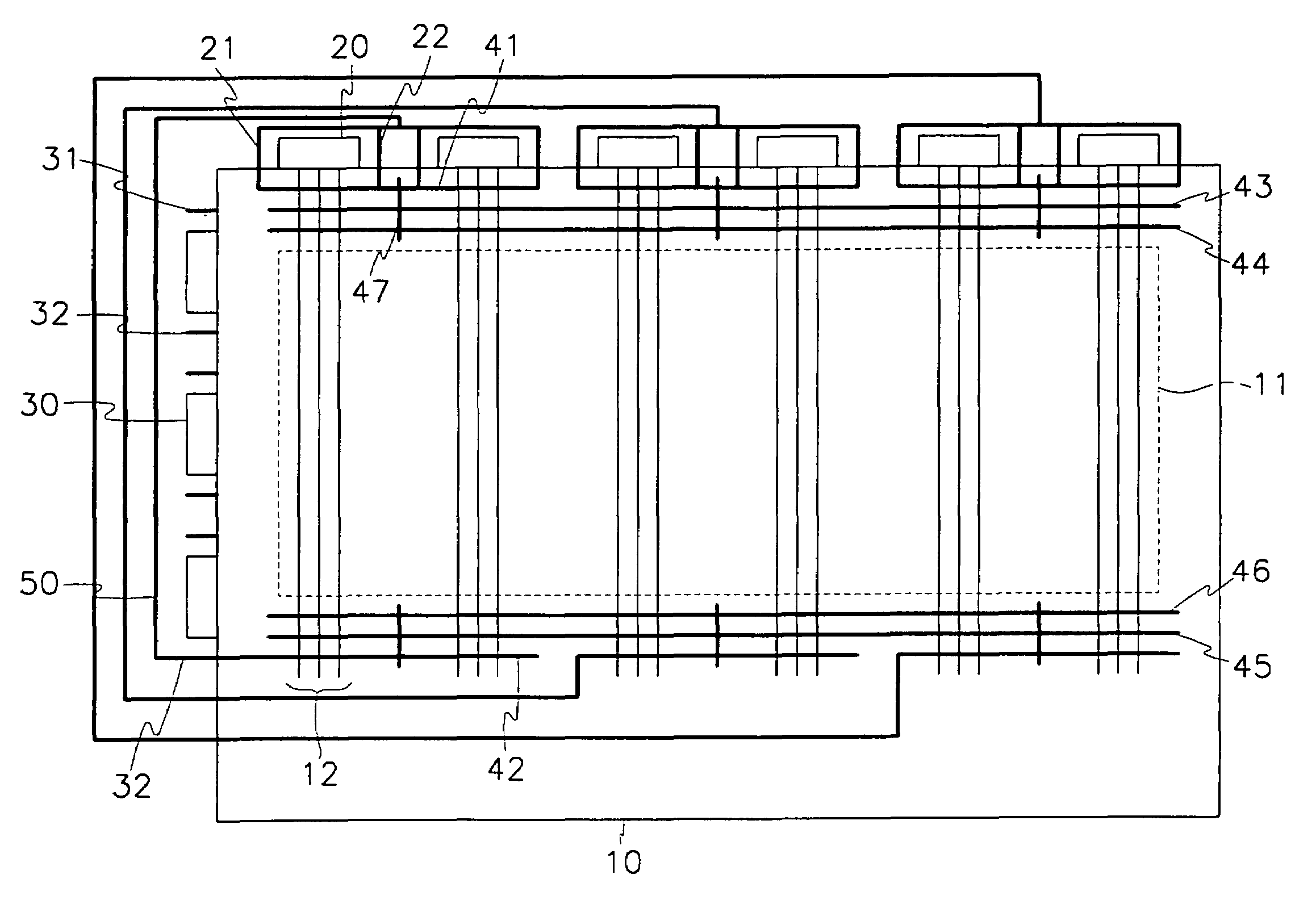
[0025]FIG. 1 is a circuit diagram of a TFT array substrate for a liquid crystal display according to a first preferred embodiment of the present invention.

[0026]As shown in FIG. 1, a plurality of data lines 12 is formed on an insulating substrate 10 in the vertical direction. A plurality of gate lines (not shown) is formed on the substrate 10 in the horizontal direction. The data lines 12 cross the gate lines to thereby form a display area 11 where pictorial images are displayed. The substrate 10 has a peripheral area externally surrounding the display area 11. The peripheral area may be roughly divided into left, right, upper and lower regions with respect to the display area 11.

[0027]Driving ICs 20 and 30 are provided at the upper and left peripheral regions of the substrate 10 such that they are connected to the data lines 12 and the gate lines, respectively. The driving IC...


PUM

PropertyMeasurementUnit
areaaaaaaaaaaa
light transmissionaaaaaaaaaa
voltageaaaaaaaaaa

Abstract

A thin film transistor array substrate for a liquid crystal display includes an insulating substrate with a display area and a peripheral area surrounding the display area. The peripheral area has an upper region above the display area and a lower region below the display area. Signal lines are formed on the substrate such that the signal lines are bundled into a plurality of blocks. Each block has a predetermined number of signal lines. A plurality of first upper repair lines is formed at the upper peripheral region of the substrate, crossing one or more blocks of the signal lines. A plurality of second upper repair lines is formed at the upper peripheral region of the substrate, crossing all of the signal lines. A plurality of first lower repair lines are formed at the lower peripheral region of the substrate, connected to the corresponding first upper repair lines. The first lower repair lines cross the signal lines crossed by the first upper repair lines. A plurality of second lower repair lines is formed at the lower peripheral region of the substrate, crossing all of the signal lines. A plurality of upper connection members crosses the first upper repair lines and the second upper repair lines. A plurality of lower connection members crosses the first lower repair lines and the second lower repair lines. In this structure, even though line breakage is concentrated at a particular area, such line breakage can be collectively repaired using the spare neighboring repair lines and interconnection lines interconnecting the repair lines efficiently.

Description

BACKGROUND OF THE INVENTION[0001](a) Field of the Invention[0002]The present invention relates to a thin film transistor (TFT) array substrate for a liquid crystal display and, more particularly, to a TFT array substrate having with repair lines.[0003](b) Description of the Related Art[0004]Generally, liquid crystal displays are structured with a color filter substrate with a common electrode and color filters, a TFT array substrate with TFTs and pixel electrodes, and a liquid crystal sandwiched between the substrates. In operation, different voltages are applied to the common electrode and the pixel electrodes to form electric fields, and under the application of the electric fields, the molecular orientation of the liquid crystal changes. This controls light transmission and displays pictorial images on the screen.[0005]The TFTs are connected to the pixel electrodes individually in order to switch the voltage applied to each pixel electrode.[0006]Gate lines for transmitting scanni...

Claims


Application Information

Patent Timeline
Patent Type & Authority Patents(United States)
IPC IPC(8): G02F1/13G02F1/1333G02F1/136H01L29/04H01L29/02H01L27/01G02F1/1362H01L21/77H01L21/84H01L27/12
CPCG02F1/1309H01L27/1214G02F1/136259H01L27/1244G02F1/136
Inventor PARK, WOON-YONG
Owner SAMSUNG DISPLAY CO LTD
Why Eureka
Try Eureka