Method for fabricating window ball grid array semiconductor package

a technology of window ball grid array and semiconductor package, which is applied in the manufacture of semiconductor/solid-state devices, electric devices, solid-state devices, etc., can solve the problems of undesired increase in fabrication cost, significant drawbacks in fabrication methods, and complicating fabrication performance, so as to increase fabrication costs, enhance mechanical strength of semiconductor packages, and facilitate fabrication

Active Publication Date: 2005-09-22
UTAC HEADQUARTERS PTE LTD
View PDF2 Cites 14 Cited by
  • Summary
  • Abstract
  • Description
  • Claims
  • Application Information

AI Technical Summary

Benefits of technology

[0014] It is a characteristic feature of utilizing a spacer having through holes sized in accordance with openings of the substrates and formed with recessed portions respectively around the through holes. During molding, the spacer is strongly clamped between the substrate and the lower mold, with the recessed portions located between the ball pads on the substrate and the edge of the openings, and the gaps between the chips and substrates and along shorter sides of the substrate openings serve as passages for the resin material to form the encapsulation body on the substrates. Besides encapsulating the chips, the resin material flows through the gaps to encapsulate the bonding wires and fill the substrate openings, the through holes of the spacer and also the gaps. The strong clamping of the spacer helps prevent flash of the resin material to the interface between the spacer and the substrate. Once if the resin material

Problems solved by technology

However, the above package fabrication method leads to significant drawbacks.
Therefore, when using substrates having openings of different sizes, new lower molds having correspondingly-dimensioned downwardly recessed cavities are required, making the fabrication cost undesirably increased.
This two-stage encapsulation process not only complicates the fabrication performance but also leads to a resin-flash problem.
During the first encapsulation process for forming the lower encapsulation body, area on the lower surface of the substrate around the opening and underneath the chip usually lacks firm support from the upper mold and is not strongly clamped by the encapsulation mold, such that the resin material injected into the downwardly re

Method used


Image

  • Method for fabricating window ball grid array semiconductor package
  • Method for fabricating window ball grid array semiconductor package
  • Method for fabricating window ball grid array semiconductor package

Examples


Embodiment Construction

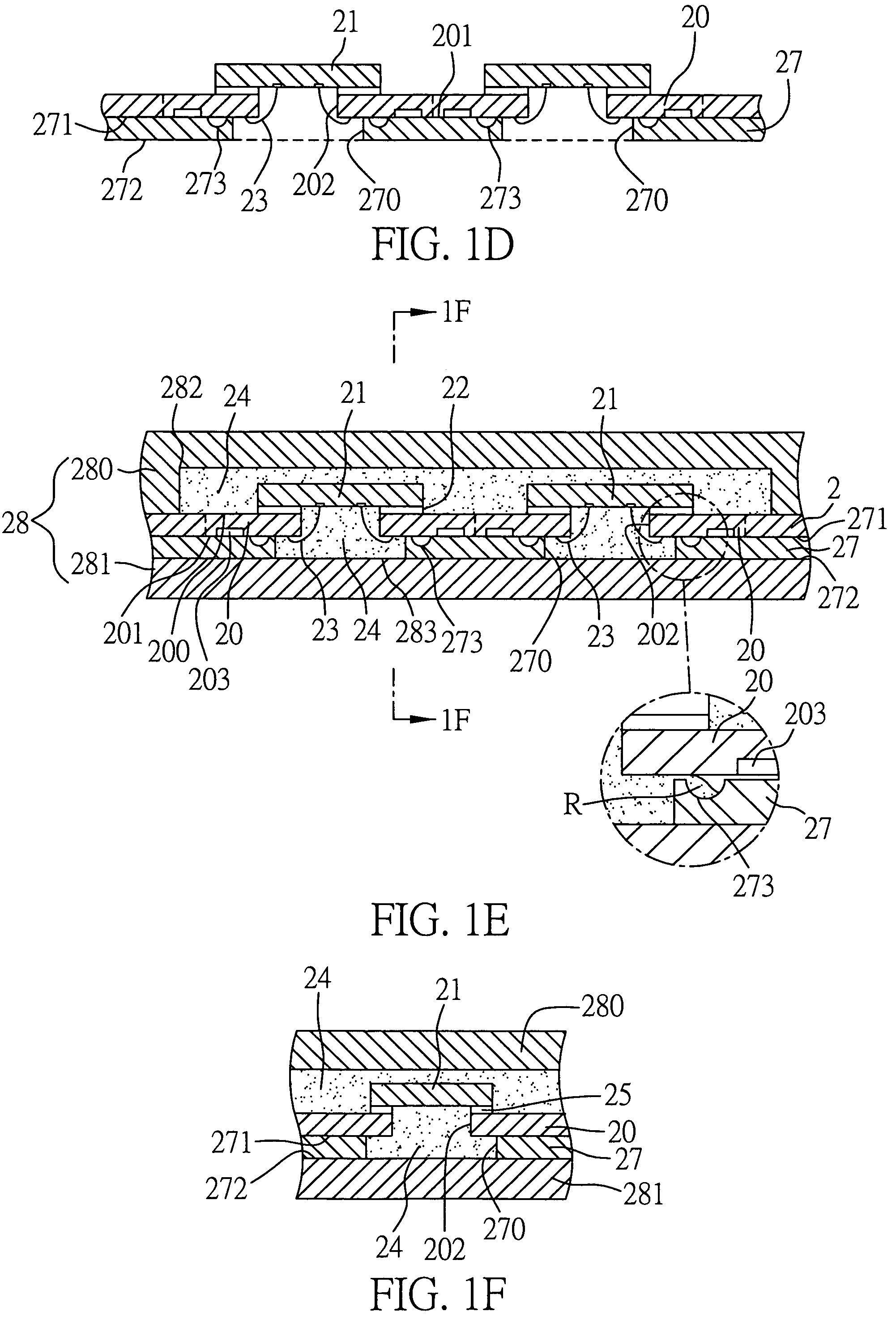
[0019] The procedural steps of a method for fabricating a window ball grid array (WBGA) semiconductor package according to the present invention are described in detail with reference to FIGS. 1A-1I.

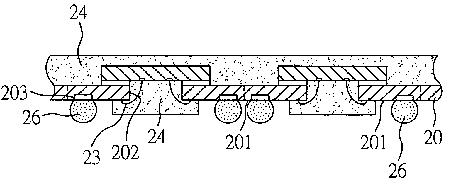
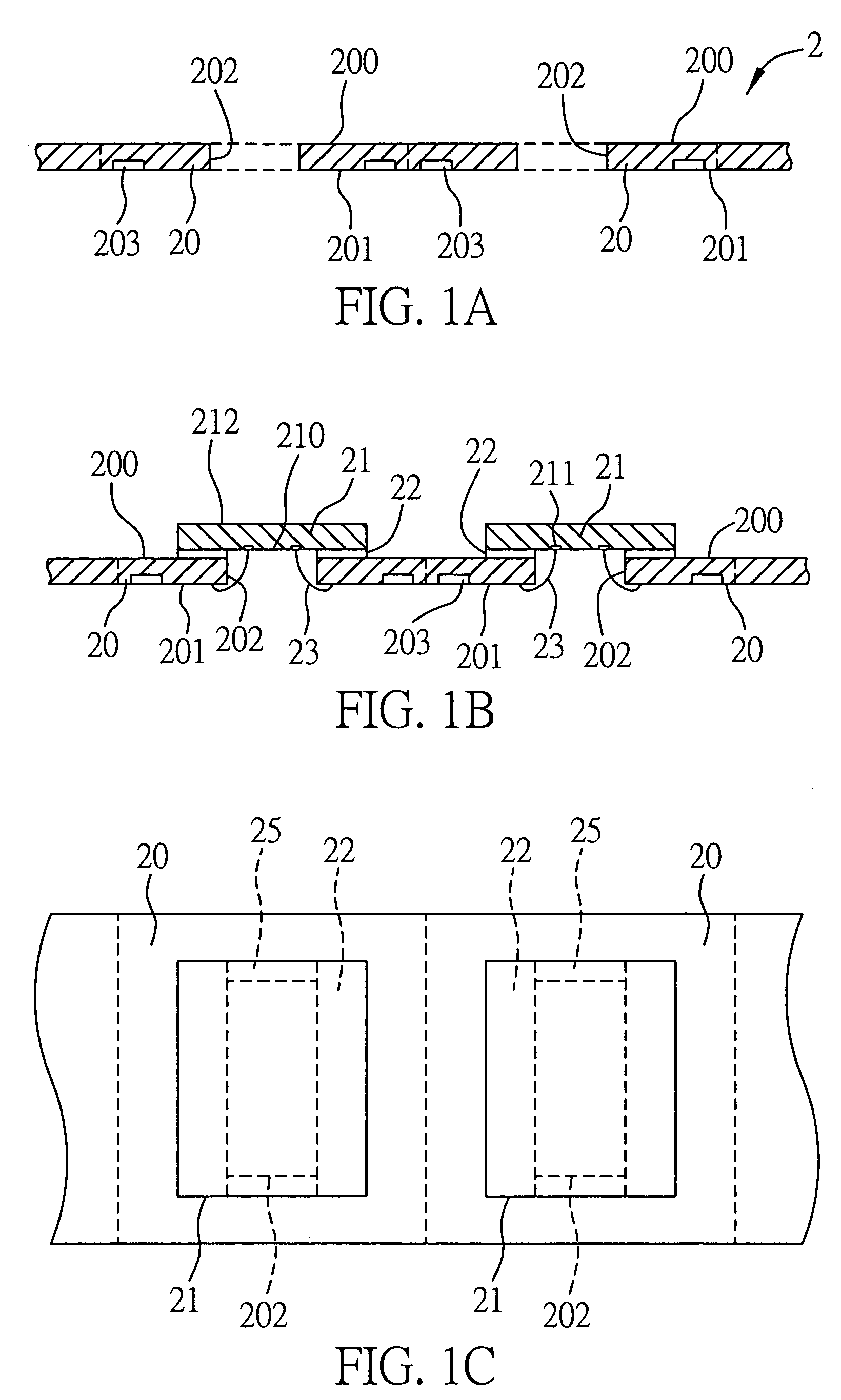
[0020] Referring to FIG. 1A, the first step is to prepare a substrate plate 2 integrally formed of a plurality of substrates 20, which can be made of a conventional resin material such as epoxy resin, polyimide resin, BT (bismaleimide triazine) resin, FR4 resin, etc. Each of the substrates 20 has an upper surface 200 and an opposite lower surface 201 and is formed with an opening 202 penetrating through the same, wherein the opening 202 preferably has a rectangular shape having two opposite longer sides and two opposite shorter sides. At least one array of ball pads 203 are formed on the lower surface 201 of each of the substrates 20 around the opening 202 and spaced apart from the edge of the opening 202. Fabrication of the substrate plate 2 employs conventional technology and is not t...


PUM


Abstract

A method for fabricating a window ball grid array (WBGA) semiconductor package is provided. A substrate is prepared having a through opening and ball pads on a lower surface thereof. A chip is mounted over the opening of the substrate via an adhesive, with gaps not applied with the adhesive left between the chip and substrate. The chip is electrically connected to the substrate via bonding wires through the opening. A spacer is attached to the lower surface of the substrate and has a through hole and a recessed portion around the through hole. During molding, the spacer is clamped between the substrate and a mold, and the recessed portion is located between the ball pads and the opening, such that a resin material for forming an encapsulation body encapsulates the chip and flows through the gaps to encapsulate the bonding wires. The recessed portion holds resin flash therein.

Description

FIELD OF THE INVENTION [0001] The present invention relates to fabrication methods of semiconductor packages, and more particularly, to a method for fabricating a window ball grid array (WBGA) semiconductor package having a chip mounted over an opening formed through a substrate and electrically connected to the substrate via bonding wires going through the opening. BACKGROUND OF THE INVENTION [0002] A window ball grid array (WBGA) package utilizes a substrate having a through opening where electrically-connecting bonding wires are received so as to reduce the package size. FIGS. 2A-2F show the procedural steps of a fabrication method of the WBGA semiconductor package. As shown in FIG. 2A (cross-sectional view) and FIG. 2B (top view), once the substrate 10 having the through opening 102 is prepared, at least one semiconductor chip 11 is mounted on an upper surface 100 of the substrate 10 and over the opening 102 by means of an adhesive 12. The adhesive 12 is usually applied along tw...

Claims


Application Information

Patent Timeline
IPC IPC(8): H01L21/56H01L21/58H01L23/13H01L23/31H01L23/498
CPCH01L21/565H01L24/48H01L23/3114H01L23/49816H01L24/97H01L2224/48091H01L2224/4824H01L2224/73215H01L2224/97H01L2924/01079H01L2924/15311H01L23/13H01L2924/01033H01L2224/32225H01L2224/85H01L2924/00014H01L2224/83H01L2924/00H01L2924/181H01L2224/45144H01L24/45H01L2924/00012H01L2224/45015H01L2924/207
Inventor KIM, SUNG-JINHORNG, CHIH-HORNGTSAI, MING-SUNGYANG, CHUNG-TA
Owner UTAC HEADQUARTERS PTE LTD
Why Eureka
Try Eureka