Fabrication method of semiconductor package with photosensitive chip

a technology of photosensitive chips and semiconductor packages, which is applied in the direction of semiconductor devices, semiconductor/solid-state device details, electrical devices, etc., can solve the problems of damage to the reliability of the semiconductor package, the clamping force between the insert portion and the substrate is not easy to properly control, and the above semiconductor package may still suffer significant drawbacks, etc., to achieve the elimination of the damage to the substrate by the use of the insert mold, the effect of reducing the cost of manufacturing

Inactive Publication Date: 2005-08-04
SILICONWARE PRECISION IND CO LTD
View PDF7 Cites 14 Cited by
  • Summary
  • Abstract
  • Description
  • Claims
  • Application Information

AI Technical Summary

Benefits of technology

[0007] An objective of the present invention is to provide a fabrication method of a semiconductor package with a photosensitive chip, without the use of an insert mold for forming an encapsulation body or dam on a substrate, such that the fabrication cost can be reduced and the fabrication processes can be simplified.
[0008] Another objective of the present invention is to provide a fabrication method of a semiconductor package with a photosensitive chip, without the use of an insert mold for forming an encapsulation body or dam on a substrate, such that resin flash can be avoided between the mold and the substrate, and the substrate can be prevented from damage by the mold.
[0009] A further objective of the present invention is to provide a fabrication method of a semiconductor package with a photosensitive chip, without the use of a conventional adhesive for attaching an encapsulation dam to a substrate, so as to prevent delamination between the dam and substrate and moisture absorption by the adhesive.
[0013] It is a characteristic feature that interposers are used in a molding process for forming the encapsulation body or dams on the substrates. The interposers are attached via their adhesive members to the substrates. The interposers are disposed in the upwardly-recessed cavity of the upper mold and between the upper mold and the substrates, such that the interposers together with the upwardly-recessed cavity define the area or space on the substrates to be filled by the resin compound to form the encapsulation body comprising interconnected dams each located on one of the substrates. As a result, instead of an insert mold used in the prior art, a conventional encapsulation mold comprising the upper mold with the upwardly-recessed cavity and the flat lower mold can be utilized in the present invention, which effectively reduces the fabrication cost and simplifies the fabrication processes, as well as the prior-art problems of resin flash and damage to the substrate by the use of the insert mold can be eliminated. After molding, the interposers can be easily removed from the substrates since the adhesive member of the interposer may be an adhesive having poor adhesion or a UV tape whose adhesive can be reduced by UV light. The interposer is cost-effective to fabricate and can be flexibly dimensioned according to the size of substrate, thereby not undesirably increasing the fabrication cost and process complexity of the semiconductor package. It is another characteristic feature that the dam formed on each of the substrate is directly in contact with the exposed peripheral portion of the core. This arrangement effectively enhances adhesion between the dam and the substrate since the dam and the core are both made of resin materials, such that no adhesive in the prior art is required for attaching the dam to the substrate, and the prior-art problems of delamination between the dam and the substrate and moisture absorption by the adhesive can be eliminated. Moreover, the interposer may protrude from edge of the solder mask layer and extend above the exposed peripheral portion of the substrate, thereby forming a portion of the opening of the solder mask layer that is defined by the interposer, the edge of the solder mask layer and the core of the substrate. This portion of the opening is relatively small in size making the resin compound quickly absorb heat from the mold and increase its viscosity when flowing to the opening and approaching the edge of the solder mask layer, such that the resin compound would not flash out of the opening and over unintended area on the substrate. As a result, the chip and bonding wires would not be mounted on flash-contaminated area of the substrate, and the reliability and electrical connection quality can be assured for the fabricated semiconductor package.

Problems solved by technology

The resin compound forming the encapsulation body is usually opaque or non-transparent, thereby making a photosensitive chip such as CMOS (complementary metal oxide semiconductor) chip that requires light for operation not suitably incorporated in such a semiconductor package.
However, the above adhesive has relatively higher moisture absorptivity; when the adhesive with the absorbed moisture is subject to a high temperature in subsequent fabrication processes, it would lead to popcorn effect and delamination between the substrate and the encapsulation dam, thereby damaging the reliability of the semiconductor package.
However, the above semiconductor package may still suffer significant drawbacks.
However, it is not easy to properly control the clamping force between the insert portion and the substrate.
If the insert portion is not sufficiently clamped on the substrate, flash of the resin compound may occur between the insert portion and the substrate and thus contaminates the area on the substrate predetermined for chip-attachment and wire-bonding.
If the insert portion is too strongly pressed on the substrate, the substrate may be structurally damaged by the insert portion.
Moreover, the insert mold is cost-ineffective to fabricate, which requires formation of the insert portion according to the size of substrate or predetermined area on the substrate to be covered by the insert portion.
In other words, if the size of substrate or area on the substrate to be covered changes, a new mold with correspondingly-sized insert portion is required, which would undesirably increase the fabrication cost and complicate fabrication processes for the semiconductor package.

Method used


Image

  • Fabrication method of semiconductor package with photosensitive chip
  • Fabrication method of semiconductor package with photosensitive chip
  • Fabrication method of semiconductor package with photosensitive chip

Examples


first preferred embodiment

[0022]FIGS. 1A to 1F show the procedural steps for the fabrication method according to a first preferred embodiment of the invention.

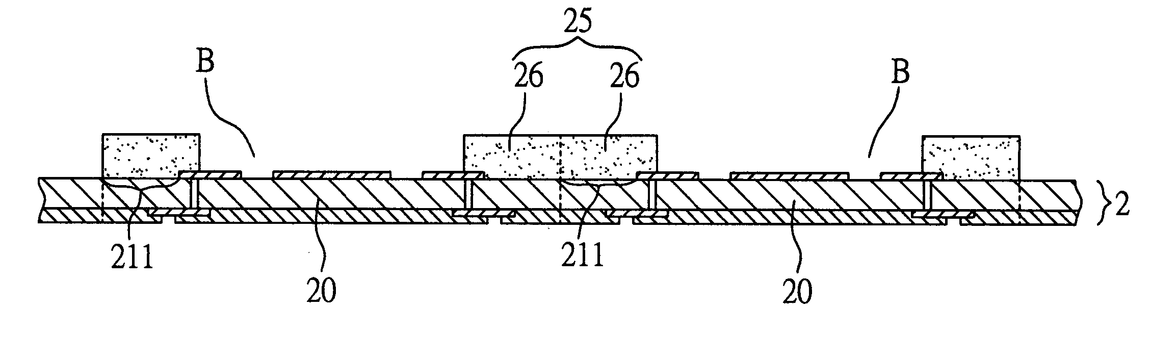
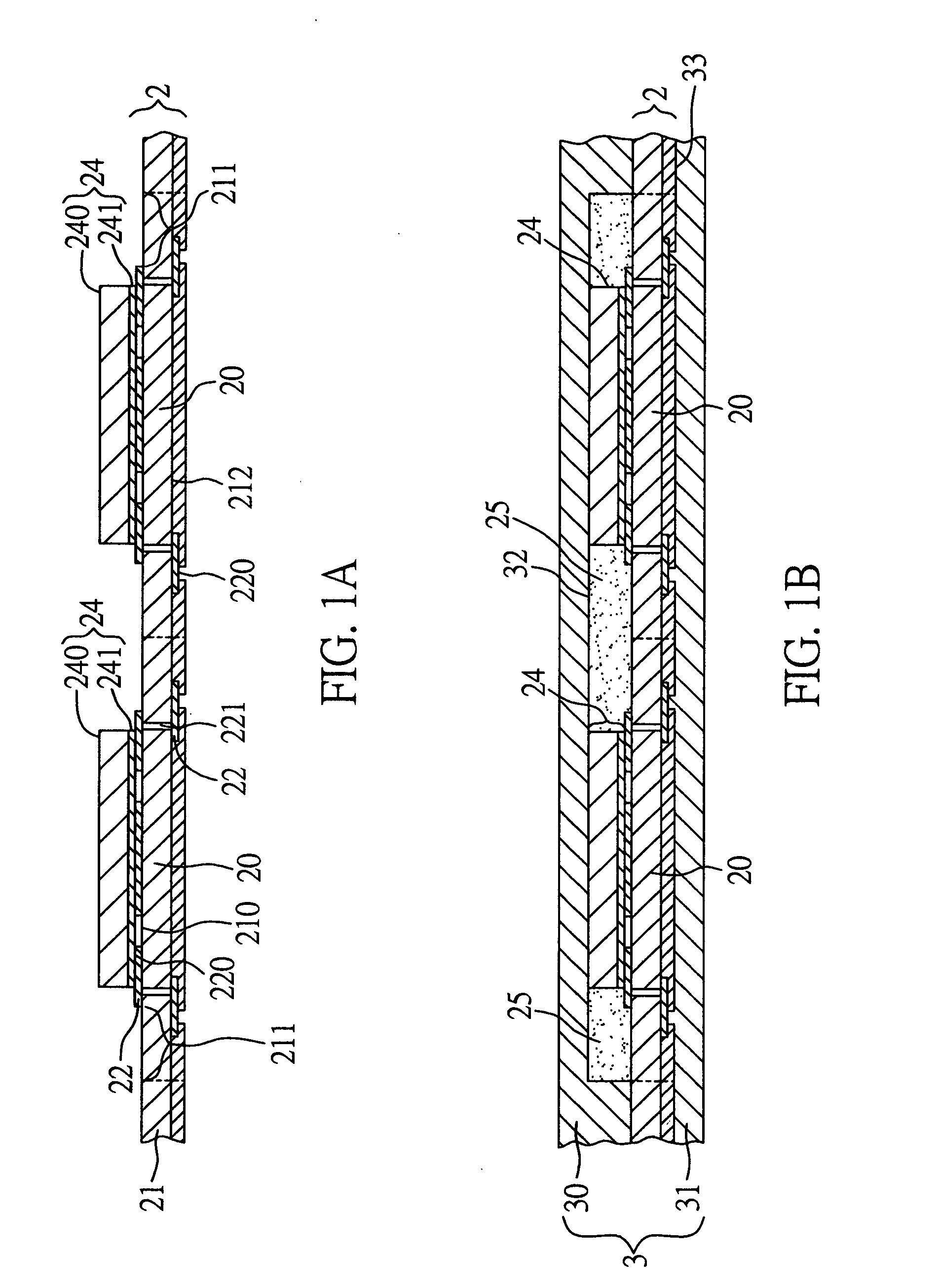
[0023] Referring to FIG. 1A, the first step is to prepare a substrate plate 2 comprising an array of substrates 20 that are integrally formed. The substrate plate 2 has a core 21 and a plurality of conductive traces 22 formed respectively on upper and lower surfaces 210, 212 of the core 21. The core 21 is primarily made of a conventional resin material such as epoxy resin, polyimide resin, BT (bismaleimide triazine) resin, FR4 resin, etc. Each of the conductive traces 22 has a terminal 220, wherein the terminals 220 on the upper surface 210 of the core 21 serve as bond fingers and the terminals 220 on the lower surface 212 of the core 21 serve as ball pads in subsequent fabrication processes. The conductive traces 22 on the upper and lower surfaces 210, 212 of the core 21 are electrically interconnected by conductive vias 221. The conductive traces 22...

second preferred embodiment

[0030]FIGS. 3A to 3E show the procedural steps for the fabrication method according to a second preferred embodiment of the invention.

[0031] Referring to FIG. 3A, the first step is to prepare a substrate plate 2′ comprising an array of integrally formed substrates 20. This substrate plate 2′ is similar in structure to the substrate plate 2 of the above first embodiment (FIG. 1A), but differs in that a solder mask layer 23 (around 25 to 50 μm thick) is applied respectively over the upper and lower surfaces 210, 212 of the core 21 and covers the conductive traces 22, and the terminals 220 of the conductive traces 22 are exposed from the solder mask layers 23. The exposed terminals 220 on the upper surface 210 of the core 21 serve as bond fingers and the exposed terminals 220 on the lower surface 212 of the core 21 serve as ball pads in subsequent fabrication processes. The solder mask layer 23 is formed an opening 230 to expose a continuous peripheral portion 211′ on the upper surfac...

third preferred embodiment

[0037]FIGS. 4A to 4E show the procedural steps for the fabrication method according to a third preferred embodiment of the invention.

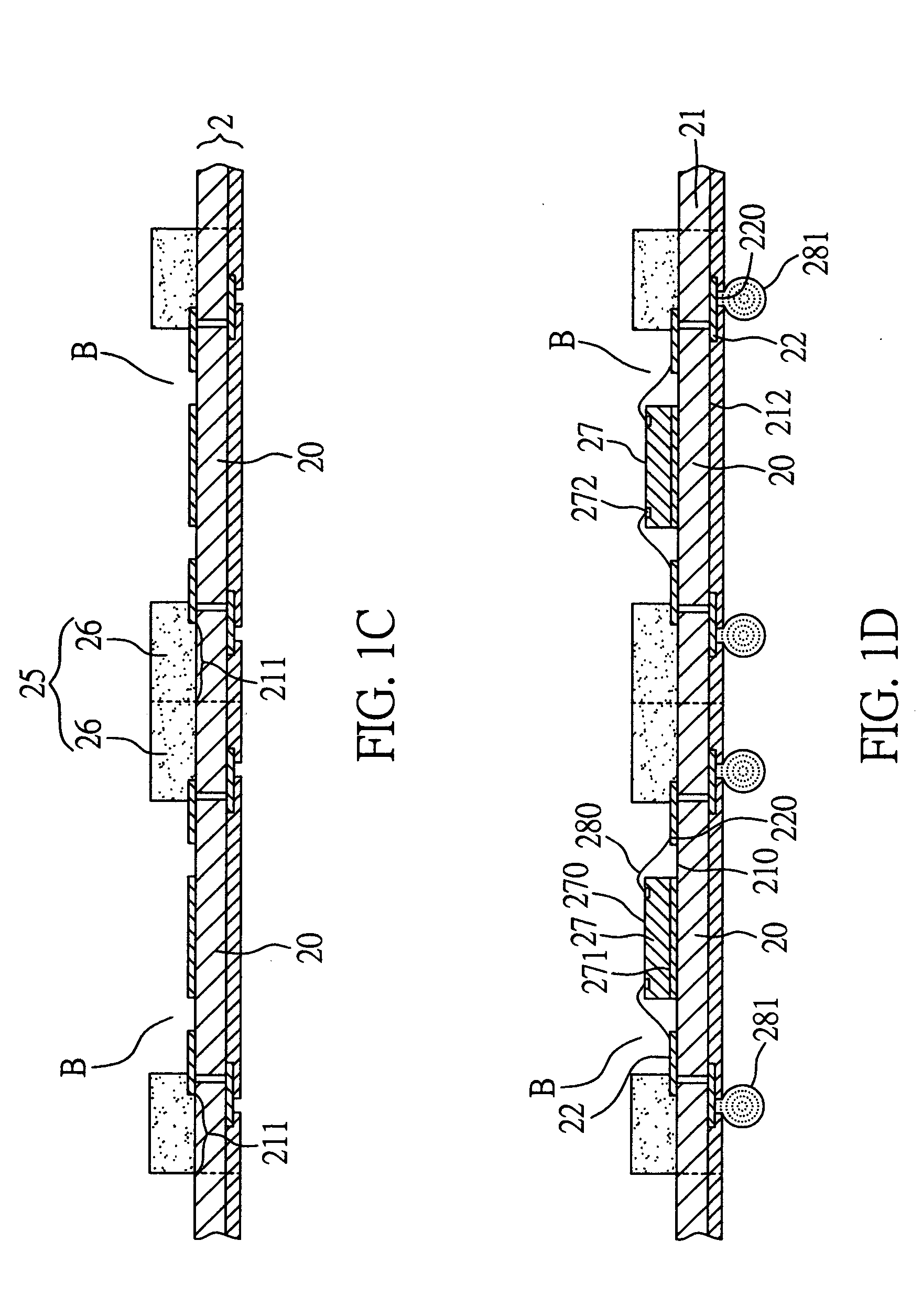
[0038] The fabrication method of this third embodiment is similar to that described in the above second embodiment, with the difference in that as shown FIG. 4A, the interposer 24 is mounted on the solder mask layer 23 on the upper surface 210 of the core 21 for each of the substrates 20 of the substrate plate 2′ in a manner that, the interposer 24 covers predetermined area for chip-attachment and wire-bonding on each substrate 20, and the interposer 24 protrudes from edge of the solder mask layer 23 and extends above the peripheral portion 211′ of the corresponding substrate 20. The interposer 24 protrudes from the edge of the solder mask layer 23 by a distance of from 0.1 to 1 mm, preferably 0.5 mm. As a result, a portion A of the opening 230 on each of the substrates 20 is formed by the interposer 24, the edge of the solder mask layer 23 and the co...


PUM


Abstract

A fabrication method of a semiconductor package with a photosensitive chip is provided. A substrate having a core is prepared. An interposer is mounted on the substrate, with a peripheral portion of the substrate exposed from the interposer. A molding process is performed and the substrate is clamped between an upper mold and a lower mold, with the interposer received in an upwardly-recessed cavity of the upper mold. A molding compound is injected into the upwardly-recessed cavity to form a dam on the peripheral portion of the substrate. Then the upper and lower molds and the interposer are removed from the substrate to expose area covered by the interposer on the substrate. At least one photosensitive chip is mounted on the exposed area of the substrate. A lid seals the dam such that the chip is received in a space defined by the substrate, the dam and the lid.

Description

FIELD OF THE INVENTION [0001] The present invention relates to fabrication methods of semiconductor packages, and more particularly, to a method for fabricating a semiconductor package incorporated with at least one photosensitive chip such as CMOS (complementary metal oxide semiconductor) chip. BACKGROUND OF THE INVENTION [0002] Semiconductor packages are electronic devices for accommodating active components such as semiconductor chips, whose structure is primarily composed of a chip mounted on a substrate and electrically connected to the substrate via conductive elements such as bonding wires, and an encapsulation body formed by a resin compound (such as epoxy resin, etc.) on the substrate to encapsulate and protect the chip and bonding wires against external moisture and contaminant. The resin compound forming the encapsulation body is usually opaque or non-transparent, thereby making a photosensitive chip such as CMOS (complementary metal oxide semiconductor) chip that require...

Claims


Application Information

Patent Timeline
Patent Type & Authority Applications(United States)
IPC IPC(8): H01L21/44H01L21/48H01L21/50H01L23/055H01L23/10H01L31/0203
CPCH01L21/50H01L23/055H01L2224/45144H01L2924/01033H01L2924/01005H01L24/48H01L2924/16195H01L2924/16152H01L2924/15311H01L2924/01082H01L2924/01079H01L2924/01029H01L2224/97H01L23/10H01L24/97H01L27/14618H01L27/14683H01L2224/16H01L2224/48091H01L2224/92247H01L2224/85H01L2924/00014H01L2224/83H01L2924/00H01L24/45H01L2224/73265H01L2924/15173H01L2924/181H01L2224/05599
Inventor HUANG, CHIEN-PINGHSIAO, CHENG-HSUHUANG, CHIH-MING
Owner SILICONWARE PRECISION IND CO LTD
Why Eureka
Try Eureka