
Method for forming wiring structure which includes annealing conductive film before and after removal of a portion of the conductive film

Inactive Publication Date: 2005-09-20
PANASONIC CORP
View PDF8 Cites 2 Cited by
  • Summary
  • Abstract
  • Description
  • Claims
  • Application Information

AI Technical Summary

Benefits of technology

[0027]In order to achieve this object, the present inventor has come up with a method for preventing the occurrence of drawbacks such as a void or a surface fracture by performing “annealing” separately “before and after a CMP process” for stepwise removal of defects contained in a conductive film to suppress the agglomeration of the defects in the conductive film that occurs in the inside or the surface of wiring during or after the annealing processes.
[0042]That is to say, with the inventive method for fabricating an electronic device, the number of annealing processes for forming a wiring structure is selectively set, so that it is possible to form a desired wiring structure, without increasing the number of processes excessively.

Problems solved by technology

However, the first and second prior arts have problems described later.
However, in the first prior art, the annealing performed on the copper film 29 causes a problem that a void (cavity) 30 is created in the copper film to be a metal wiring layer as shown in FIG.
As a result, the wiring resistance increases, thus reducing the yield of the semiconductor device and also degrading the reliability of the semiconductor device.
As a result, these surface defects act as paths for surface diffusion of copper atoms, thus greatly deteriorating resistance to electromigration.

Method used


Image

  • Method for forming wiring structure which includes annealing conductive film before and after removal of a portion of the conductive film
  • Method for forming wiring structure which includes annealing conductive film before and after removal of a portion of the conductive film
  • Method for forming wiring structure which includes annealing conductive film before and after removal of a portion of the conductive film

Examples


embodiment 1

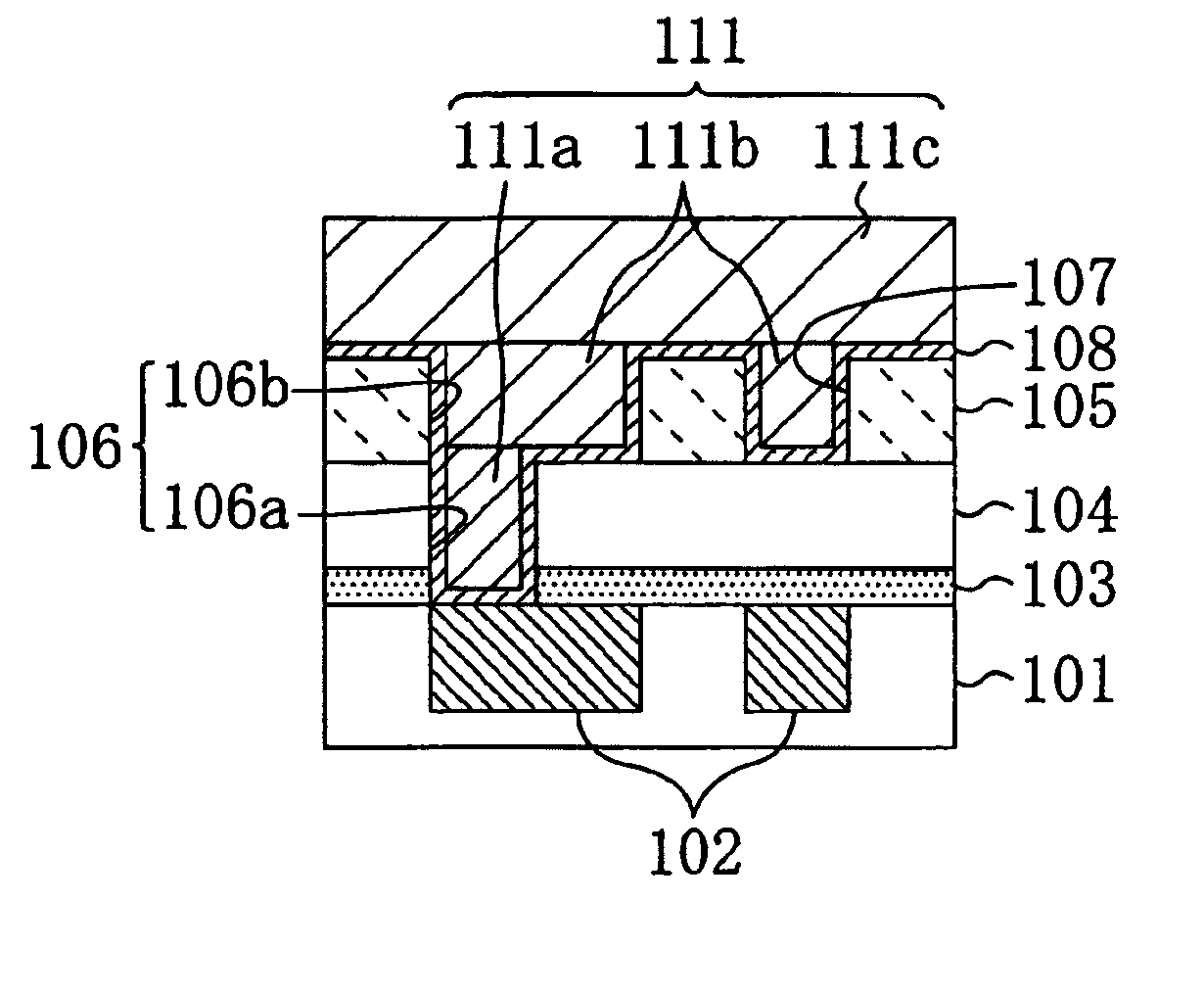
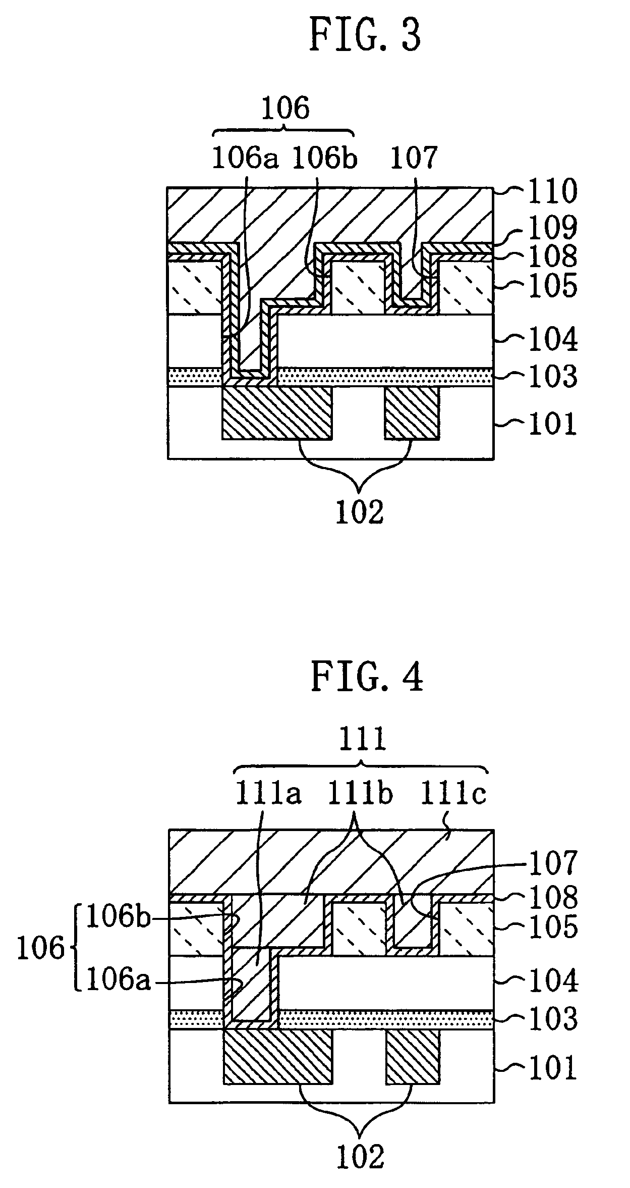
[0055]Hereinafter, a method for fabricating an electronic device according to a first embodiment of the present invention will be described with reference to the drawings. This embodiment is characterized in that an annealing process is performed on a copper (Cu) film to serve as wiring one time “before a CMP process” and one time “after the CMP process”.

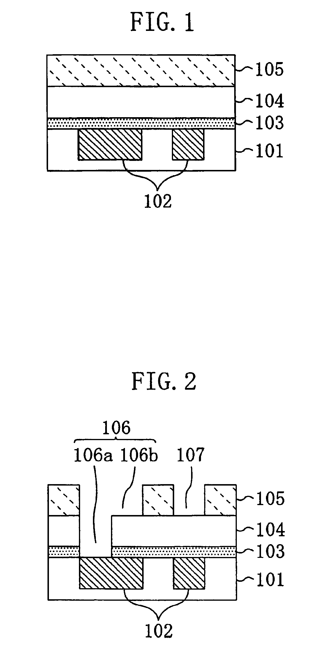
[0056]FIGS. 1 through 7 are cross-sectional views showing respective process steps of a method for fabricating an electronic device of the first embodiment.

[0057]First, as shown in FIG. 1, a lower wiring layer 102 is formed in an insulating film 101 deposited over, for example, a semiconductor substrate (not shown), and then the surface of the insulating film 101 in which the lower wiring layer 102 has been buried is planarized. Then, an SiN film 103, a SiO2 film 104 and a FSG film 105 are deposited in this order by, for example, a CVD process over the planarized insulating film 101 and the lower wiring layer 102.

[0058]Next, as show...

embodiment 2

[0079]Hereinafter, a method for fabricating an electronic device according to a second embodiment of the present invention will be described with reference to the drawings. This embodiment is characterized in that the number of annealing processes for forming a wiring structure is selectively set in accordance with the width of a recess to be a wiring groove, for example. This embodiment has such a feature because of the following reasons.

[0080]Specifically, in most of the multilevel wiring structures, the wiring width is smaller at lower-level wiring and the wiring width is relatively larger in upper-level wiring in general. Accordingly, if wiring is formed by burying conductive films in, for example, wiring grooves, drawbacks such as voids are more liable to occur at lower-level wiring with narrow wiring grooves. In addition, since annealing processes are performed in forming respective upper-level wirings, lower-level wiring is subjected to the plurality of annealing processes ac...


PUM


Abstract

A recess is formed in an insulating film, and then a conductive film is deposited over the insulating film so as to fill the recess. Thereafter, the conductive film is subjected to a first heat treatment. Subsequently, part of the conductive film located outside the recess is removed, and then the remaining part of the conductive film is subjected to a second heat treatment with the surface thereof exposed.

Description

BACKGROUND OF THE INVENTION[0001]The present invention relates to methods for forming wiring structures in electronic devices such as semiconductor devices.[0002]Examples of known methods for forming wiring structures include a first prior art (see, for example, Japanese Laid-Open Publication No. 2000-277520) in which heat treatment (hereinafter, referred to as annealing) is performed before a chemical mechanical polishing (CMP) process and a second prior art (see, for example, Japanese Laid-Open Publication No. 11-186261) in which annealing is performed after a CMP process. Hereinafter, these two major known methods for forming wiring structures will be described with reference to the drawings with the case where wire is formed in a wiring groove formed in an insulating film taken an example.[0003]FIGS. 9A through 9F are cross-sectional views showing respective process steps of a method for forming a wiring structure according to the first prior art in which “annealing” is performe...

Claims


Application Information

Patent Timeline
IPC IPC(8): H01L21/70H01L21/02H01L21/768H01L21/321
CPCH01L21/3212H01L21/76807H01L21/76882H01L21/76886H01L2221/1036
Inventor HARADA, TAKESHI
Owner PANASONIC CORP
Learn More