
Display device and apparatus using same

a technology applied in the field of display device and display device using the same, can solve the problems of increasing the power consumption together with the increase in the operating speed, increasing the speed of the circuit structure, and increasing the cost of ic/sub>s that operate at high speed, so as to reduce the capacitance of the data-holding circuit, low parasitic capacitance between the electroconductive layer of the apparatus and the data-holding circuit, and low parasitic capacitance

Active Publication Date: 2007-05-24
NEC LCD TECH CORP
View PDF18 Cites 9 Cited by
  • Summary
  • Abstract
  • Description
  • Claims
  • Application Information

AI Technical Summary

Benefits of technology

[0018] An object of the present invention is to provide a display device and an apparatus having the display device, in which size of the display device can be reduced because the controller IC and interface circuit are formed on the same substrate as the display device substrate, the circuit surface area can be made smaller and power consumption can be reduced by decreasing the capacitance of the memory cells, the operational reliability of the memory unit can be increased, and costs can be made lower, in any cases when the display data of all the pixels is sent serially to the liquid crystal module with high-speed transfer and without high-speed transfer for each frame time interval.
[0019] The display device of the present invention is a display device in which a data-holding circuit having a capacitance, and a display portion having a plurality of pixel electrodes are formed on a single first carrier substrate, wherein a second carrier substrate disposed opposite the first carrier substrate is placed above the display portion, but the opposing substrate is not present above the area in which the data-holding circuit is disposed. In the present invention, the parasitic capacitance of the data-holding circuit is low because there is no carrier substrate facing the data-holding circuit. As a result, the capacitance of the data-holding circuit can be reduced in the case of a fixed ratio between the parasitic capacitance and the capacitance of the memory cell and the like within the data-holding circuit. Since the capacitance of the data-holding circuit is small, the area required for the layout of the data-holding circuit is also small.

Problems solved by technology

And for high speed transfer, the driver IC also must operate at higher speed, a through-current or the like is generated in the large number of CMOS (Complementary Metal Oxide Semiconductor) components constituting the circuit elements, and power consumption increases together with the increase in operating speed.
ICs that operate at high speed also have higher cost.
The complexity and transfer speed of the circuit structure then increases when the gradation increases, leading to further increases in power consumption and higher costs.
More specifically, since the price and power consumption of the driver IC increase together with higher definition and higher gradation of displays, there is a problem in that the number of pixels and gradations is limited because the power consumption and price of the system overall must be limited.
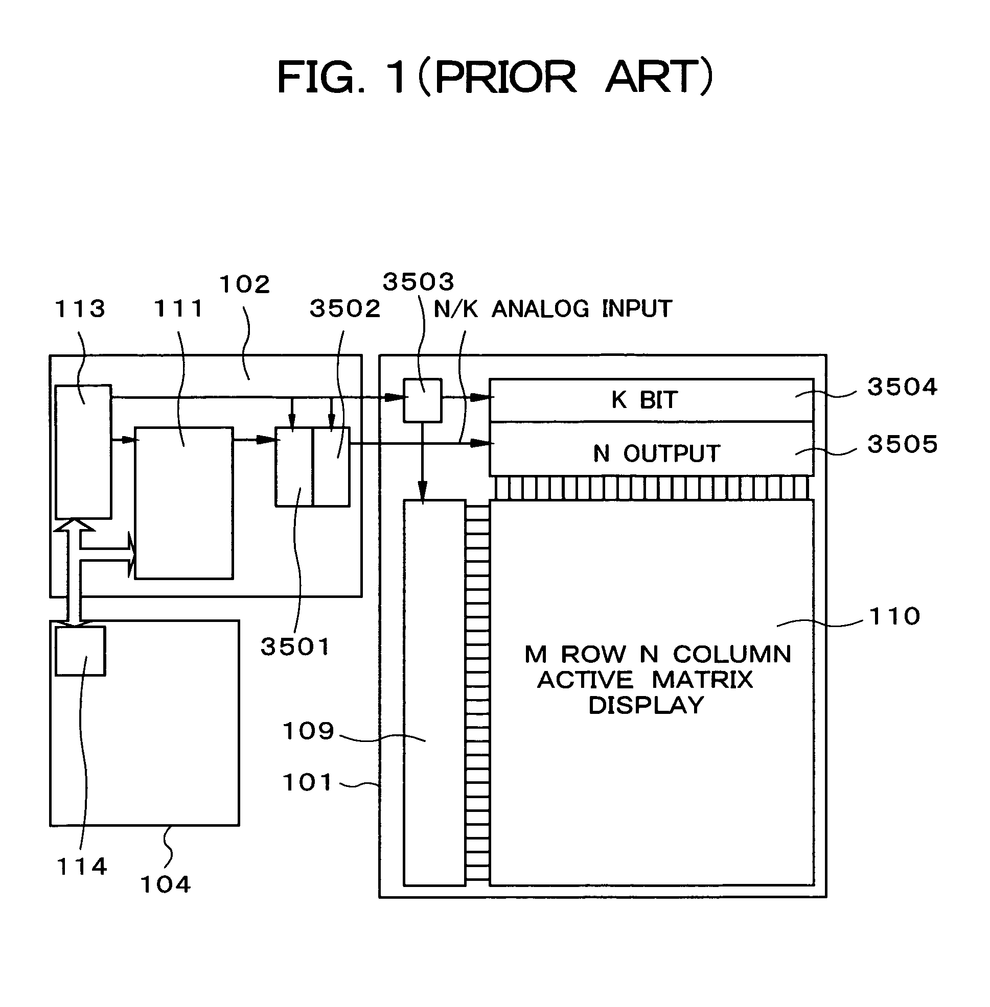
The voltages used in the circuit blocks on the display device substrate 101 are different, and there is therefore a problem in that it is necessary to jointly use processes that are suited to a plurality of voltages, and costs in the manufacturing process increase.
The drive circuit-integrated liquid crystal display devices also have a problem in that the size of the display device cannot be reduced because the controller IC and interface circuit 114 are mounted outside the display device substrate.
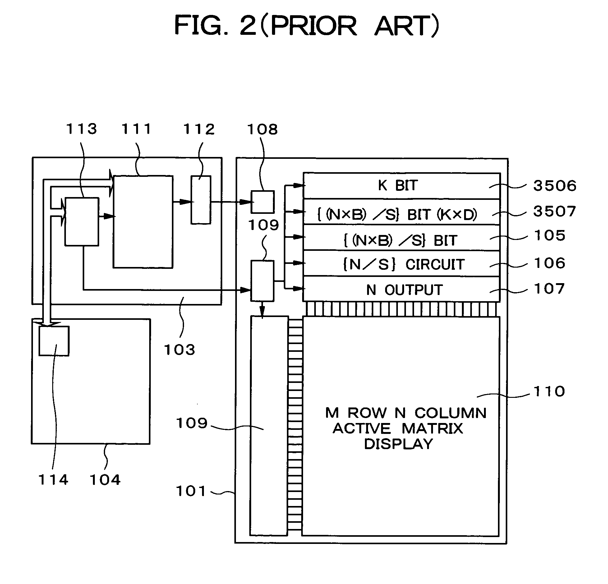
In this manner, the prior application achieves the initial objects, but in a structure in which memory is integrated on the carrier substrate, it is difficult to reduce the parasitic capacitance of the bit lines.
Therefore, there is a limit to reducing the capacitance of the memory cells and it is difficult to reduce the circuit surface area of the frame memory.
As a result, it is difficult to reduce the size of display devices that use the frame memory.
Also, this technology requires a considerable amount of electric current for charging and discharging because the capacitance of the memory cells is high.
Electric potential is reduced due to wiring resistance because the circuit surface area is large, and power consumption is high due to charging and discharging of the parasitic capacitance of the wiring, leading to a limitation to the amount by which power consumption can be reduced.

Method used


Image

  • Display device and apparatus using same
  • Display device and apparatus using same
  • Display device and apparatus using same

Examples


first embodiment

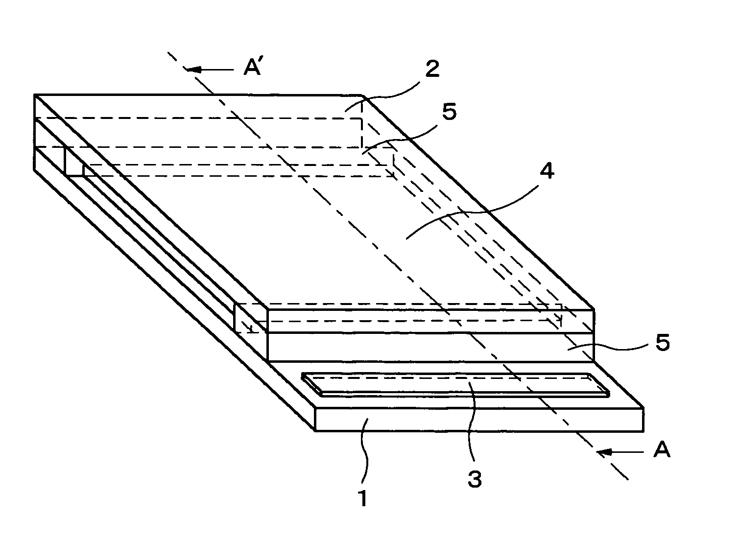
[0056] The embodiments of the present invention are described in detail below with reference to the attached diagrams. FIG. 3A is a perspective view showing the display device of the present invention, and FIG. 3B is a cross-sectional diagram along line A-A′ of FIG. 3A. A display area 4 and a data-holding circuit 3 provided with a capacitance (not shown) are aligned in parallel at regular intervals on a first carrier substrate 1. A spacer 5 is formed with greater thickness than that of the display area 4 along the side nearest to the data-holding circuit 3 of the display area 4 and the side facing thereto without making contact with the data-holding circuit 3 and without being present further outward from the edge portion of the first carrier substrate 1.

[0057] A second carrier substrate 2 facing the first carrier substrate 1 is disposed above the display area 4, and a fixed interval is provided by the spacer 5 between the first carrier substrate and the second carrier substrate. Ho...

third embodiment

[0068] Based on this structure, optical leakage current and other adverse effects are unlikely to occur even if an area of the data-holding circuit 3 is irradiated with light from the side facing the second carrier substrate 2, in the same manner as in the third embodiment described above. Also, if for any reason optical leakage current occurs, the magnitude of the leakage current is far less than when a light-blocking film 6 is not present. Since the light-blocking film 6 is formed from a nonconductive body, the parasitic capacitance that accompanies the capacitance of the data-holding circuit 3 is also low. As a result, the capacitance of the data-holding circuit 3 can be reduced in the case of a fixed ratio between the capacitance of the data-holding circuit 3 and the parasitic capacitance that accompanies the data-holding circuit 3. Since the capacitance of the data-holding circuit 3 can be reduced, the area required for the layout of the data-holding circuit 3 is small.

fourth embodiment

[0069] In the same manner as the fourth embodiment described above, the parasitic capacitance that accompanies the capacitance of the data-holding circuit 3 can be reduced by selecting a dual-frequency driven liquid crystal having a crossover frequency of several megahertz as the medium that is disposed between the first carrier substrate 1 and second carrier substrate 2 in the vicinity of the data-holding circuit 3.

[0070] The sixth embodiment of the present invention is described next. FIG. 7A is a perspective view showing the display device of the sixth embodiment of the present invention, and FIG. 7B is a cross-sectional diagram along line A-A′ of FIG. 7A. In FIG. 7, the same reference numerals are assigned to the same constituent elements as FIGS. 3 to 5, and a detailed description thereof is omitted. In the fifth embodiment described above, a nonconductive light-blocking film 6 is disposed in the area facing the data-holding circuit 3 on the surface of the second carrier substr...


PUM


Abstract

A display device has a data-holding circuit with a capacitance and a display portion with a plurality of pixel electrodes, formed on a first carrier substrate. In the display device, a second carrier substrate disposed opposite the first carrier substrate is placed above the display portion, but the opposing substrate is not present above the area in which the data-holding circuit is disposed. The parasitic capacitance of the data-holding circuit can thereby be reduced. Therefore, the capacitance in the data-holding circuit can be reduced and the area required can be reduced as well. The display data of all the pixels is sent serially to the liquid crystal module without high-speed transfer for each frame time interval, and size can be reduced because the controller IC and interface circuit are formed on the same substrate as the display device substrate.

Description

CROSS REFERENCE TO RELATED APPLICATIONS [0001] This application claims foreign priority of Japanese Patent Application No. 2005-336426, filed Nov. 21, 2005. BACKGROUND OF THE INVENTION [0002] 1. Field of the Invention [0003] The present invention relates to a display device used in projectors, laptop PCs, monitors, mobile phones, PDAs, and the like, and to an apparatus that uses this display device. [0004] 2. Description of the Related Art [0005] Conventionally, drive circuits and various other circuits in display devices are configured with an LSI or the like that is made by using silicon technology, and are disposed outside of the display device. However, as technology has developed in recent times, the drive circuits and various other circuits have come to be mounted on a carrier substrate of the display devices, and display devices mounted with these circuits are being brought into practical use. A known example of a display device with such a circuit internally mounted is a dis...

Claims


Application Information

Patent Timeline
Patent Type & Authority Applications(United States)
IPC IPC(8): G09G3/36
CPCG02F1/13454G09G3/3611G09G2300/0408G09G2330/021G09G2360/18G11C7/1006G11C7/1012G11C7/1051G11C11/4091G11C11/4093G11C11/4096G09G3/3648G09G2310/0294
Inventor TAKATORI, KENICHIHAGA, HIROSHI
Owner NEC LCD TECH CORP
Learn More